
Atomic layer junction oxide and preparing method thereof

a technology of atomic layer junction and atomic layer, which is applied in the direction of polycrystalline material growth, chemistry apparatus and processes, and growth of polycrystalline materials, etc., can solve the problems of high efficiency of epiaxial growth, easy movement of photons, and fundamental limitations of conventional photo diodes, etc., to achieve high light absorption efficiency, and photocharge separation

Active Publication Date: 2017-10-10
RES & BUSINESS FOUND SUNGKYUNKWAN UNIV
View PDF3 Cites 0 Cited by
  • Summary
  • Abstract
  • Description
  • Claims
  • Application Information

AI Technical Summary

Benefits of technology

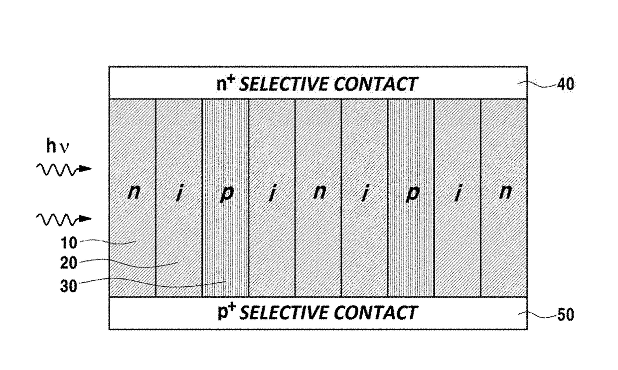
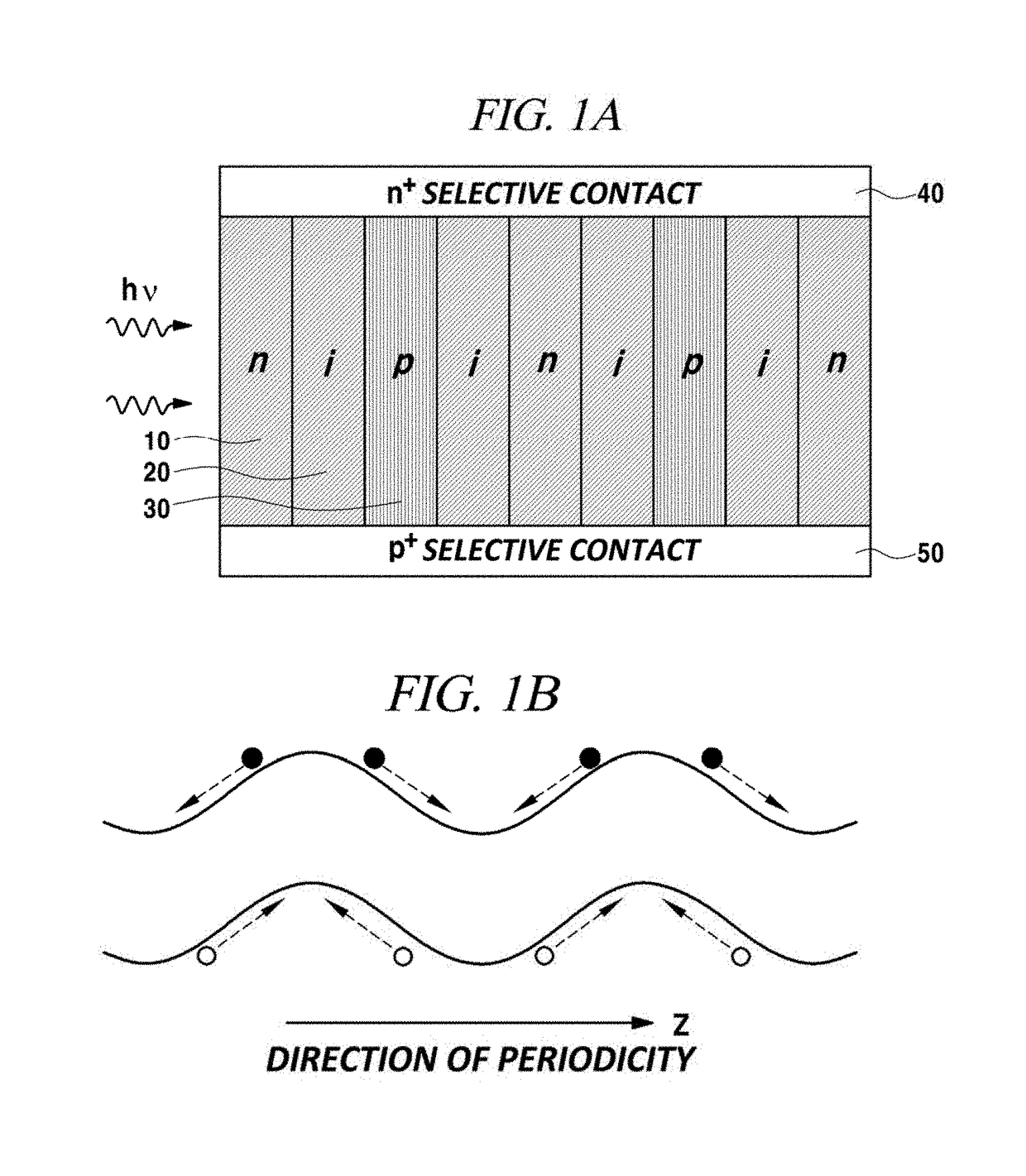
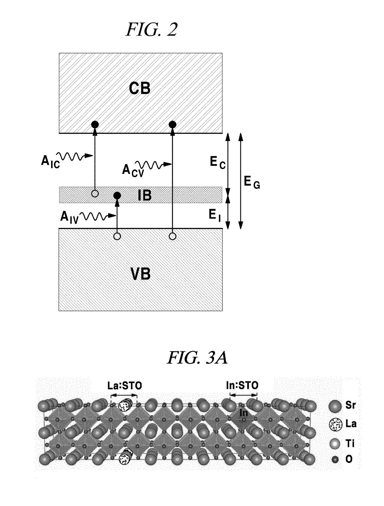
This patent discusses a method of making an atomic layer junction oxide that has high light absorption efficiency in sunlight. By adjusting the effective band gap of the oxide, photons can be absorbed from a valence band to an intermediate band, and from the intermediate band to a conduction band. The entire layer of oxide can have a valence band to conduction band energy band bending, which improves photocharge separation and collection efficiency. Overall, the method allows for improved performance of photoelectric conversion devices.

Problems solved by technology

However, in order to implement a photo diode with a multijunction of heteromaterials, a complicated manufacturing process is needed, and, an interface defect may easily occur at a junction interface due to a lattice mismatch, which results in that a dangling bond of an interface defect induces recombination of electron and hole so that there is a limitation in materials suitable for a lattice match that induces epitaxial growth for high efficiency.
Therefore, the conventional photo diode structure has a fundamental limitation in that only electron and hole generated by photons can be easily moved at a junction interface by a potential difference.
Meanwhile, graphene, which is the most well known as a two-dimensional material, does not have a band gap by Klein tunneling and thus cannot be applied as a material of a photo diode.

Method used


Image

  • Atomic layer junction oxide and preparing method thereof
  • Atomic layer junction oxide and preparing method thereof
  • Atomic layer junction oxide and preparing method thereof

Examples


examples

[0085]Method of Calculating Electronic Configuration

[0086]An electronic configuration of an atomic layer junction oxide suggested in the present Example was calculated using the density functional theory (DFT) code of VASP (vienna ab-initio simulation package). For simulation of the n-i-p-i structure, 2×2×10 supercells having a perovskite structure with 200 atoms and having a lattice constant of 3.904 Å were used in calculation. In this case, each of an n-type doped oxide atomic layer and a p-type doped oxide atomic layer had a thickness of 1 unit cell and each intrinsic oxide atomic layer had a thickness of 4 unit cells. The materials used in the n-i-p-i structure were formed as La:SrTiO3—SrTiO3—In:SrTiO3—SrTiO3, La:SrTiO3—SrTiO3—N:SrTiO3—SrTiO3, and La:SrTiO3—SrTiO3—Sr:La MnO3—SrTiO3.

[0087]A pseudopotential was calculated using the Projector Augmentaed Wave (PAW) method of the local density approximation (LDA). Some core electrons were included in a pseudopotential of a metal elem...


PUM

PropertyMeasurementUnit
cut-off energyaaaaaaaaaa
wavelengthsaaaaaaaaaa

Abstract

Provided are an atomic layer junction oxide, a method of preparing the atomic layer junction oxide, and a photoelectric conversion device including the atomic layer junction oxide. The atomic layer junction oxide can include an n-type doped atomic layer oxide; an intrinsic atomic layer oxide; a p-type doped atomic layer oxide; and an intrinsic atomic layer oxide.

Description

CROSS-REFERENCE TO RELATED APPLICATIONS[0001]This application claims the benefit of Korean Patent Application No. 10-2015-0093549 filed on Jun. 30, 2015, the entire disclosure of which is incorporated herein by reference.TECHNICAL FIELD[0002]The present disclosure relates to an atomic layer junction oxide, a method of preparing the atomic layer junction oxide, and a photoelectric conversion device including the atomic layer junction oxide.DESCRIPTION OF RELATED BACKGROUND ARTS[0003]A photo diode has been widely used as a photoelectric conversion device by using a p-n junction, in which a DC voltage is generated by photovoltaic effect due to electron and hole generated by a photon absorbed by a junction layer of the photo diode. As new renewable energy becomes more important socially due to global warming and depletion of fossil fuels, expectations of a photoelectric conversion device capable of directly converting clean and inexhaustible solar energy into electric energy has been in...

Claims


Application Information

Patent Timeline
Patent Type & Authority Patents(United States)
IPC IPC(8): H01L31/0352C30B29/32C30B29/68H01L31/032H01L31/105H01L31/18H01L31/036
CPCH01L31/035263C30B29/32C30B29/68H01L31/18H01L31/036H01L31/105H01L31/032
Inventor LEE, JAICHANCHUNG, BONGWOOK
Owner RES & BUSINESS FOUND SUNGKYUNKWAN UNIV
Learn More