Crucible for growing sapphire single crystal, and method for producing crucible for growing sapphire single crystal
a technology crucible, which is applied in the direction of charging supports, lighting and heating apparatus, furniture, etc., can solve the problem of difficult growth of sapphire single crystal
- Summary
- Abstract
- Description
- Claims
- Application Information
AI Technical Summary
Benefits of technology
Problems solved by technology
Method used
Image
Examples
example 1
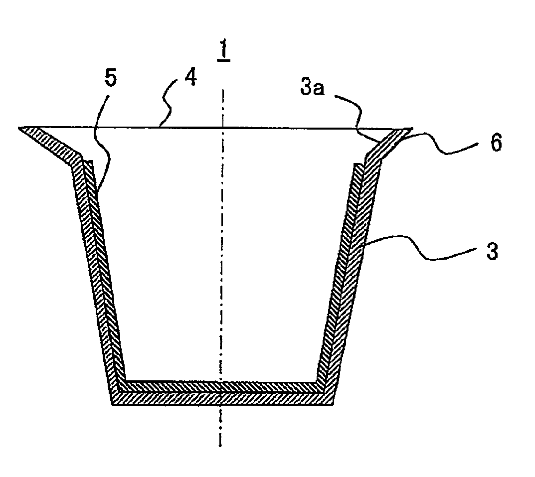
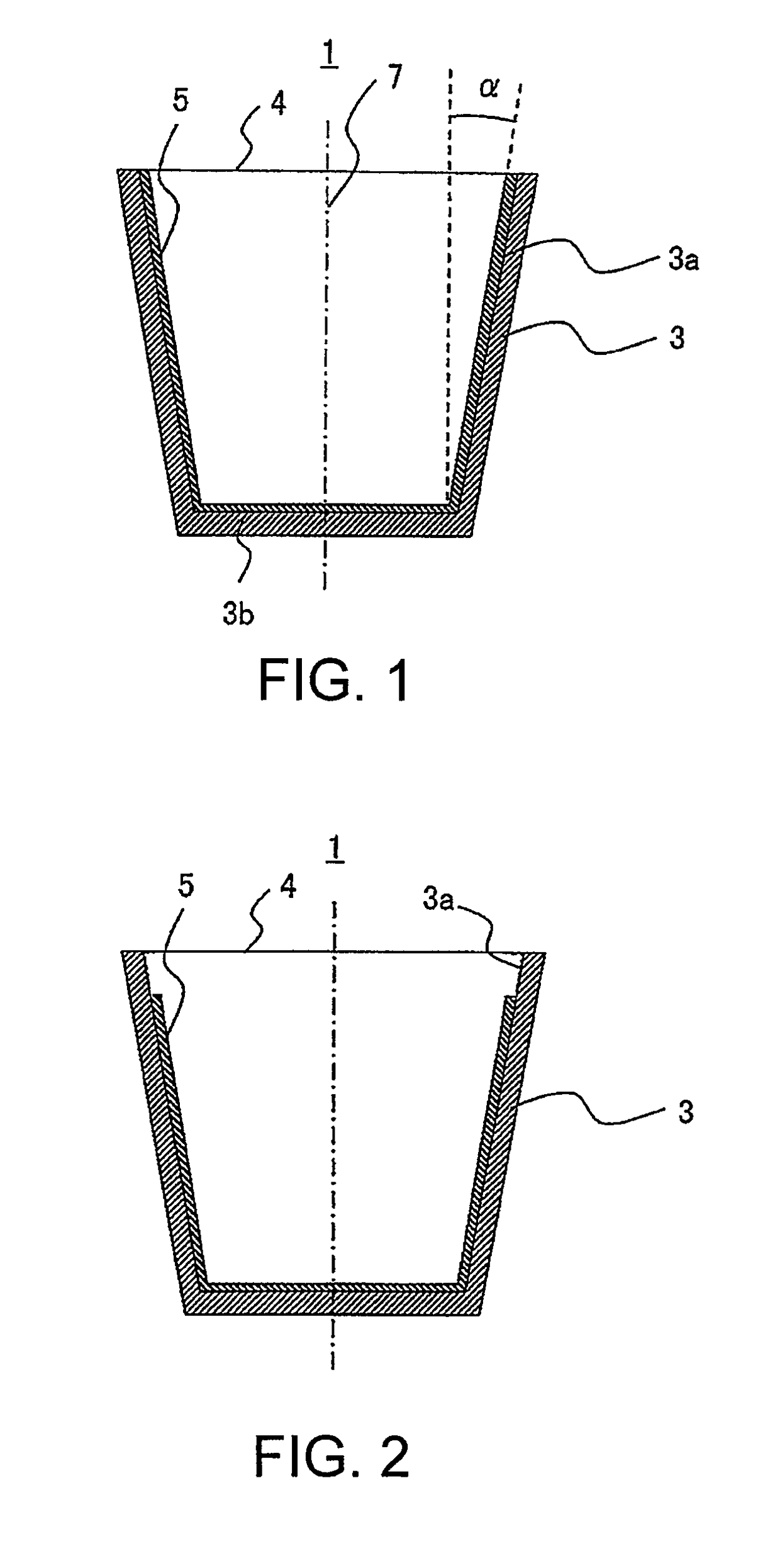
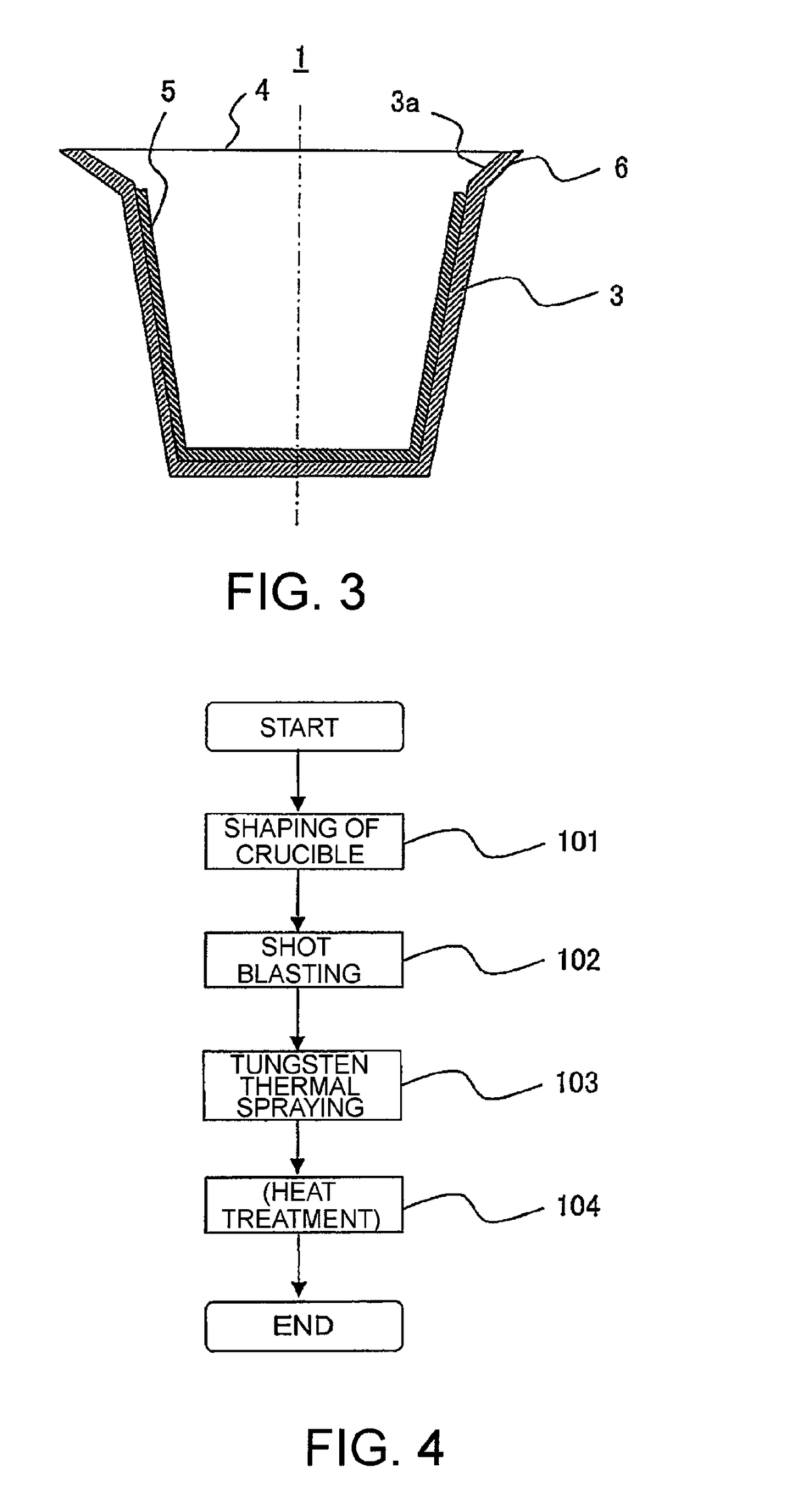
[0104]The crucible 1 for growing a sapphire single crystal in which the coating layer 5 was formed by the thermal spraying method was produced and used to melt sapphire, followed by cooling, and then an attempt was made to take sapphire out of the crucible. A specific process is as described below.
[0105]
[0106]First, as a preliminary test, a crucible smaller than dimensions to which this invention was assumed to be applied was produced and used to melt alumina (sapphire raw material), and a comparison in ease of separation was made on the basis of surface roughness.
[0107]Specifically, first, a molybdenum small crucible having a diameter of 20 mm and a depth of 20 mm was prepared, and the inner periphery of the base material 3 was subjected to shot blasting with alumina particles passing through a 20-mesh sieve (opening size: 864 μm) or passing through a 60-mesh sieve (opening size: 221 μm). After that, the coating layer 5 was formed on the inner periphery of the base material 3 by th...
example 2
[0131]In Example 1, a base material obtained by doping Mo with 0.3 to 2 mass % of lanthanum oxide, and intermittently dispersing the oxide along processing morphology to form a partial fibrous morphology was used as the base material 3, the coating layer 5 was formed, and an attempt was made to grow a sapphire single crystal. FIG. 8 to FIG. 10 show examples of observation results of the cross-section of the base material 3. It should be noted that FIG. 8 to FIG. 10 are the results of photographing with EPMA-1720H at an acceleration voltage of 15 kV, FIG. 8 shows the distribution of La, FIG. 9 shows a back scatter electron (BSE) image showing the morphology of Mo, and FIG. 10 shows a Mo base.
[0132]Next, with the use of this base material, a molybdenum crucible for growing sapphire having a diameter of 400 mm, a height of 400 mm, and a thickness of 5 mm was used to melt alumina (sapphire raw material) and a comparison in ease of separation was made on the basis of the cross-sectional ...
example 3
[0134]The sample of Example 1 was photographed with EPMA-1720H at an acceleration voltage of 15 kV, and an evaluation was made as to whether or not the particles used in the shot blasting (20 mesh in this example) remained between the base material 3 and the coating layer 5. FIG. 11 shows the result.
[0135]As shown in FIG. 11, the particles used in the shot blasting were observed as white spots.
[0136]The result revealed that the particles used in the shot blasting remained between the base material 3 and the coating layer 5, indicating that it was preferred to remove the particles.
PUM
| Property | Measurement | Unit |
|---|---|---|
| surface roughness Ra | aaaaa | aaaaa |
| surface roughness Ra | aaaaa | aaaaa |
| thickness | aaaaa | aaaaa |
Abstract
Description
Claims
Application Information


