Logic circuit, semiconductor device, electronic component, and electronic device

a logic circuit and semiconductor technology, applied in logic circuits, power consumption reduction, pulse techniques, etc., can solve the problems of data loss more severe problems in dynamic logic circuits, etc., to reduce power consumption, reduce the number of elements, and increase the effect of operation speed

Inactive Publication Date: 2018-04-03
SEMICON ENERGY LAB CO LTD
View PDF145 Cites 6 Cited by
  • Summary
  • Abstract
  • Description
  • Claims
  • Application Information

AI Technical Summary

Benefits of technology

[0005]An object of one embodiment of the present invention is to provide a novel semiconductor device or a method for operating the novel semiconductor device. Another object of one embodiment of the present invention is to reduce power consumption, to reduce the number of elements, to increase operation speed, to change the voltage of an output signal, and the like.
[0017]One embodiment of the present invention can provide a novel semiconductor device or a method for operating the novel semiconductor device. For example, one embodiment of the present invention can reduce power consumption, reduce the number of elements, increase operation speed, or change the voltage of an output signal.

Problems solved by technology

Operation of dynamic logic circuits implies to store data temporarily; thus, leakage current from transistors causes more severe problems in dynamic logic circuits than in static logic circuits.
When leakage current from transistors is large, the data stored in the dynamic logic circuits is lost.

Method used


Image

  • Logic circuit, semiconductor device, electronic component, and electronic device
  • Logic circuit, semiconductor device, electronic component, and electronic device
  • Logic circuit, semiconductor device, electronic component, and electronic device

Examples


embodiment 1

[0054]In this embodiment, a dynamic logic circuit is described as an example of a semiconductor device.

>

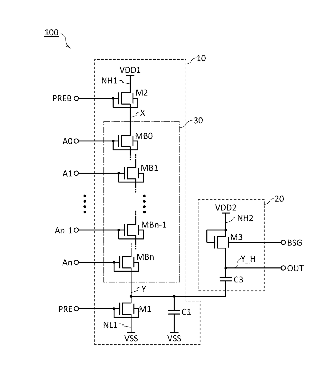
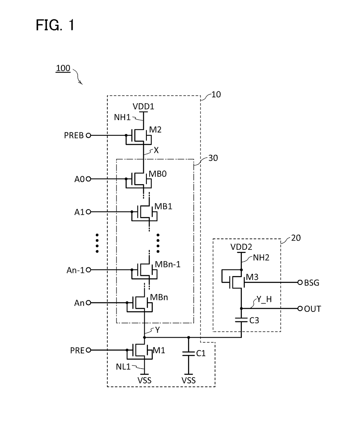
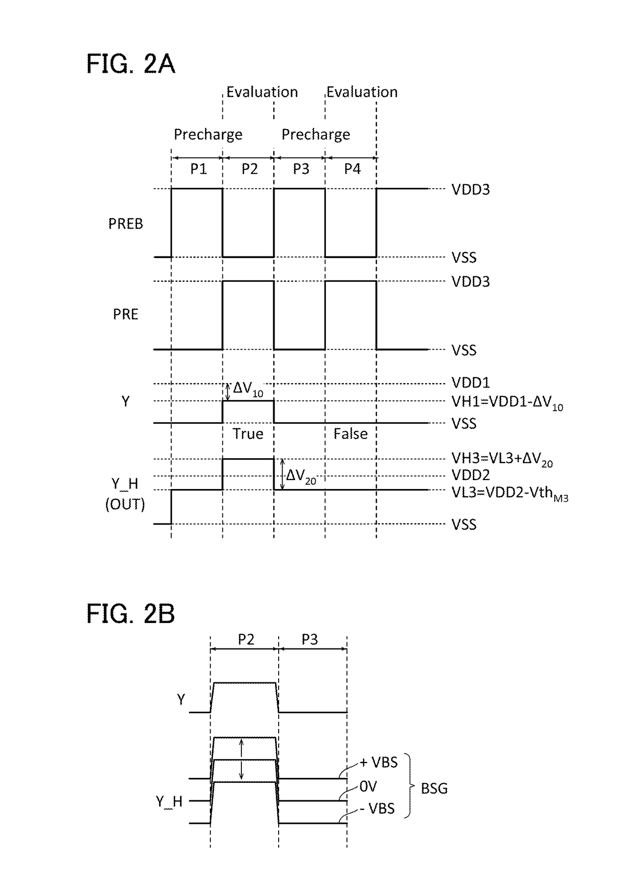
[0055]FIG. 1 is a circuit diagram showing an example of the dynamic logic circuit. A logic circuit 100 in FIG. 1 is a dynamic logic circuit that can output a signal OUT having a logic level determined by n+1 signals A0 to An (n is an integer of 1 or more). The logic circuit 100 includes a dynamic logic circuit 10 and a circuit 20. VSS, VDD1, and VDD2 are supplied to the logic circuit 100. VSS represents low power supply voltage. VDD1 and VDD2 represent high power supply voltages. Here, VDD2>VDD1>VSS is satisfied.

10>

[0056]The dynamic logic circuit 10 is a logic circuit having n+1 inputs. The dynamic logic circuit 10 includes a circuit 30, a transistor M1, a transistor M2, a capacitor C1, and nodes X, Y, NH1, and NL1. Here, the node Y functions as an output node of the dynamic logic circuit 10.

[0057]The node NL1 can function as a power supply node on the low level side to which VSS ...

embodiment 2

[0109]In this embodiment, a semiconductor device including the logic circuit of Embodiment 1 is described.

[0110]There are known semiconductor devices that include a circuit array including a plurality of circuits arranged in array, wirings corresponding to the arrangement of the circuits, and peripheral circuits for driving the circuit array. As a peripheral circuit for driving the circuits in the circuit array, the dynamic logic circuit of Embodiment 1 can be used.

[0111]Typical examples of the semiconductor devices include a memory device in which a plurality of memory cells are arranged in array (e.g., a dynamic random access memory (DRAM), a static random access memory (SRAM), or a flash memory), an imaging device having a plurality of pixels (an imaging element), and an active matrix display device having a plurality of pixels (e.g., a liquid crystal display device, an electroluminescence (EL) display device, or a MEMS display device). Examples of such semiconductor devices are ...

example 4

Device Structure Example 4

[0143]Although the OS transistor of the memory device 300 has a similar device structure to that of the transistor 500 and the Si transistor is a FIN-type transistor in the above examples, the device structures of the OS transistor and the Si transistor included in the memory device 300 are not limited to the above examples. For example, the OS transistor can be a transistor having a device structure similar to that of a transistor 502 (FIGS. 32A to 32D). Furthermore, the Si transistor can be a planar-type transistor. Such an example is shown in FIG. 15.

[0144]In the example in FIG. 15, the layer 350 is stacked over the layer 352, and the layer 351 is stacked over the layer 350. The memory cell array 301 is formed using the memory cells 313. Here, a transistor Mn2 and a transistor Mp2 are an n-channel Si transistor and a p-channel Si transistor, respectively. FIG. 15 illustrates a cross-sectional structure of the transistor MW3 in the channel length directio...


PUM


Abstract

The drive capability of a logic circuit is improved. The logic circuit includes a first output node, a dynamic logic circuit, a diode-connected first transistor, and a capacitor. The dynamic logic circuit includes a second output node and a plurality of second transistors forming and evaluation circuit. The first transistor and the plurality of second transistors all have one of an n-type conductivity and a p-type conductivity. One terminal of the capacitor is electrically connected to the first output node. The other terminal of the capacitor is electrically connected to the second output node. A first terminal of the first transistor is electrically connected to the first output node. A first voltage is input to a second terminal of the first transistor. The voltage of the first output node is changed by a voltage applied to a back gate of the first transistor.

Description

BACKGROUND OF THE INVENTION[0001]1. Field of the Invention[0002]One embodiment of the present invention disclosed in the specification, the drawings, and the claims of this application (hereinafter referred to as “this specification and the like”) relates to a logic circuit, a semiconductor device such as a processing device, a driving method thereof, a manufacturing method thereof, and the like. One embodiment of the present invention is not limited to the shown technical field. For example, one embodiment of the present invention relates to a memory device, a processing device, an imaging device, a display device, a light-emitting device, a power storage device, a driving method thereof, or a manufacturing method thereof.[0003]2. Description of the Related Art[0004]Logic circuits can be classified into static logic circuits, dynamic logic circuits, pseudo logic circuits, and the like. Operation of dynamic logic circuits implies to store data temporarily; thus, leakage current from...

Claims


Application Information

Patent Timeline
Patent Type & Authority Patents(United States)
IPC IPC(8): H03K19/00H03K19/017H01L29/786
CPCH03K19/0013H03K19/017H01L29/7869H01L27/1225H03K17/063H03K19/0948H03K19/0963
Inventor TAMURA, HIKARU
Owner SEMICON ENERGY LAB CO LTD
Why Eureka
Try Eureka