Solar cell and solar cell unit

Inactive Publication Date: 2006-12-26
SEIKO EPSON CORP
View PDF13 Cites 5 Cited by
  • Summary
  • Abstract
  • Description
  • Claims
  • Application Information

AI Technical Summary

Benefits of technology

[0011]This makes it possible to provide a solar cell which can secure current and voltage of practically required levels, that is, a solar cell which is excellent in the photoelectric conversion efficiency.
[0040]Moreover, in this solar cell unit, it is also preferred that at least one of the first and second electrodes, arranged at the side from which solar rays enter, has a top surface, and a light catalyst made of titanium dioxide (TiO2) is coated on or placed on the top surface. According to this structure, it possible to degrade impurity substances (such as deoxidized carbon, and organic matters) by the light catalyst, even in the case where the solar cell unit is used out-doors, it is possible to prevent the surfaces of the first sand or second electrode from being contaminated in a preferred manner.

Problems solved by technology

Due to this structure, the dye-sensitized solar cell is subject to many problems in that, for example, leakage of electrolyte solution is liable to occur when the sealing is broken and the like.
Therefore, the dye-sensitized solar cell cannot have a practical life as a solar cell.
Further, current and voltage of practically required levels cannot be secured by simply employing a flat-shaped titanium electrode because of its small absorption area of solar rays.

Method used


Image

  • Solar cell and solar cell unit
  • Solar cell and solar cell unit
  • Solar cell and solar cell unit

Examples


first embodiment

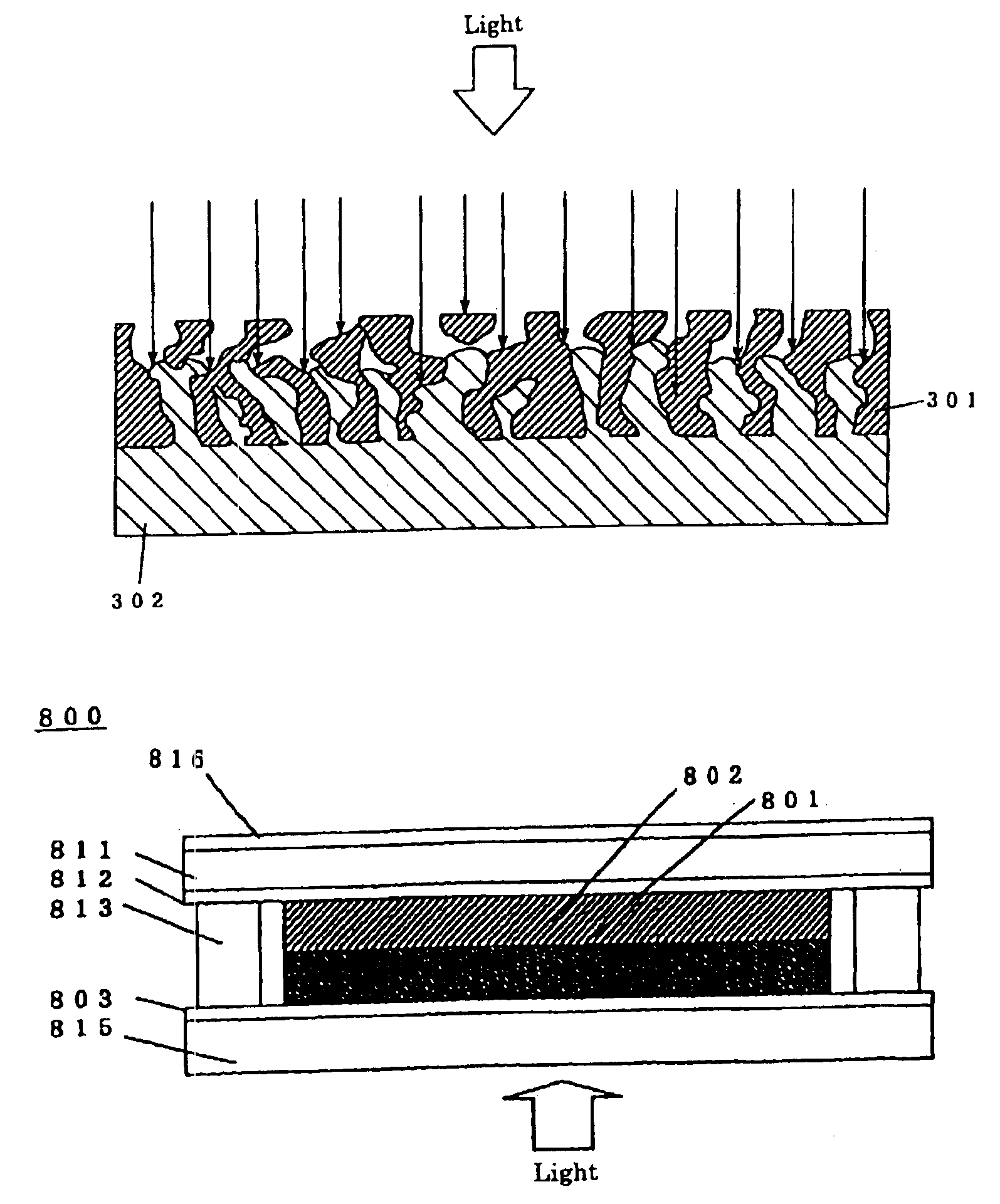
[0052]FIG. 1 is an illustration which schematically shows the structure of a solar cell (solar cell unit) 100, which is an embodiment of a solar cell employing a semiconductor according to the present invention.

[0053]The solar cell 100 includes a first substrate 104, such as a glass substrate or a metal substrate, and a first electrode 103 formed on the first substrate 104. The first electrode 103 is formed from a transparent electrode mask of ITO or the like or a metallic electrode (which is made of a metal selected from the group consisting of Al, Ni, Cr, Pt, Ag, Au, Cu, Mo, Ti and Ta, an alloy containing any one or more of these metals, or a compound containing any one of these metals).

[0054]An anatase type titanium dioxide (TiO2) semiconductor 101 is formed on the first electrode 103. The titanium dioxide (TiO2) semiconductor is an n-type semiconductor.

[0055]A comb-shaped (stripe-like) second electrode 102 is formed on the anatase type titanium dioxide (TiO2) semiconductor 101. ...

second embodiment

[0085]While the normal titania semiconductor reacts with only the ultraviolet rays in solar rays as described above, the titania semiconductor of the present invention is subjected to the processing for sensitizing to absorption wavelength of rays, such as solar rays, so as to be able to react with the rays up to the visible ray region.

[0086]Specifically, examples of such processing include (1) a method in which dye is adsorbed on the porous surface of the titania semiconductor (the dye adsorption method), (2) a method in which oxygen defects are formed in the titania to reduce the band gap in order to sensitize to the visible rays (the oxygen defect method), and (3) a method in which the titania is doped with a very small quantity of impurities (the impurity doping method), and so forth, and one kind of, or two or more kinds of, these methods can be used alone or in combination with other method.

[0087]First, the first method (the dye adsorption method) will hereinbelow be described...

third embodiment

[0102]Next, the method of forming the titania semiconductor films 101, 201 of the present invention will hereinbelow be described in detail.

1 Powder Molding Method

[0103]The titania semiconductor employed in the present invention is formed by utilizing what is referred to as Powder Injection Molding method (in general, it is called the PIM Method), or what is referred to as Metal Injection Molding Method (in general, it is called the MIM method).

[0104]In these methods, a resin binder of 99 to 50% in the volume ratio is added to titanium fine powder, having the particle size of about 20 to 2,000 nm, and then they are kneaded to form a source compound, having the low viscosity (in the range of 1,000 to 3,000 P) with which the injection molding can be carried out.

[0105]At this time, Cr or V is added thereto in order to increase the absorption wavelength width of rays. This may be added to the source compound, either in the state of the oxide of Cr (CrO3), or in the state of the oxide of...


PUM


Abstract

The solar cell of the present invention includes a titanium dioxide semiconductor that is held between a pair of electrodes so that the titanium dioxide semiconductor and at least one of the electrodes form a rectification barrier.

Description

BACKGROUND OF THE INVENTION[0001]The present invention relates to a semiconductor, a solar cell employing the semiconductor, a method of manufacturing the solar cell, and a solar cell unit employing the solar cell.DESCRIPTION OF THE RELATED ART[0002]For the approximately the past ten years, grate attention has been paid to solar cells (solar batteries) employing silicon as a power source which is harmless to the environment. As for these solar cells employing silicon, a monocrystalline silicon type solar cell is known, which is used in artificial satellites or the like. In addition, a practical application of a solar cell is also known employing polycrystalline silicon (single crystal silicon) and a solar cell employing amorphous silicon. These solar cells have already been practically used in industrial and household applications.[0003]However, since these solar cells employing silicon are manufactured through a vacuum process, such as a CVD (chemical vapor deposition) process or t...

Claims


Application Information

Patent Timeline
IPC IPC(8): H01L31/00H01G9/20H01L31/06H01L31/04H01L31/07H01L35/24H01L51/44H01M14/00
CPCH01G9/2031H01G9/2068H01L31/07Y02E10/542Y02E10/549H10K85/344H10K30/83H01L31/06H01L31/04H10K30/151
Inventor FUJIMORI, YUJIMIYAMOTO, TSUTOMU
Owner SEIKO EPSON CORP
Why Eureka
Try Eureka