Memory cell and manufacturing method

A memory unit cell and polysilicon technology, which is applied in semiconductor/solid-state device manufacturing, transistors, electrical components, etc., can solve the problems of excessive component size and insufficient charge storage period, and achieve the effect of size reduction

Active Publication Date: 2008-09-03
TAIWAN SEMICON MFG CO LTD
View PDF4 Cites 0 Cited by
  • Summary
  • Abstract
  • Description
  • Claims
  • Application Information

AI Technical Summary

Problems solved by technology

[0010] The purpose of the present invention is to overcome the defects of the existing memory cells, and provide a memory cell for DRAM with a new structure. The problem of excessive component size and insufficient charge storage period makes it more suitable for practical use
[0011] Another object of the present invention is to overcome the defects of existing methods for manufacturing memory cells, and provide a new method for manufacturing memory cells. The technical problem to be solved is to reduce the memory capacity of conventional DRAMs. The problem that the cell process is not compatible with the standard CMOS process, so it is more suitable for practical use

Method used


Image

  • Memory cell and manufacturing method
  • Memory cell and manufacturing method
  • Memory cell and manufacturing method

Examples


Embodiment Construction

[0072] In order to further explain the technical means and effects of the present invention to achieve the intended purpose of the invention, below in conjunction with the accompanying drawings and preferred embodiments, the specific implementation, structure, manufacturing method, steps, Features and their functions are described in detail below.

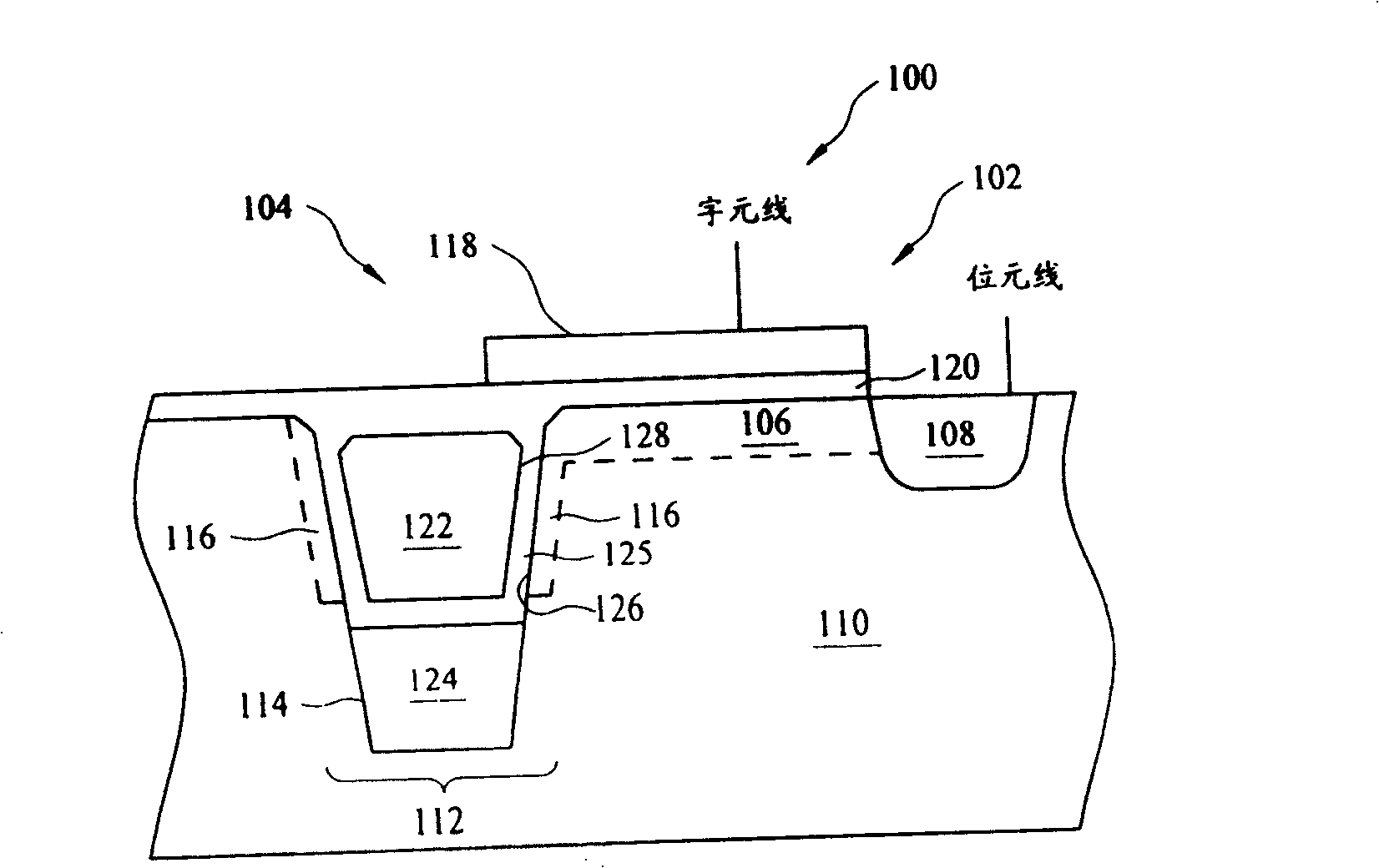
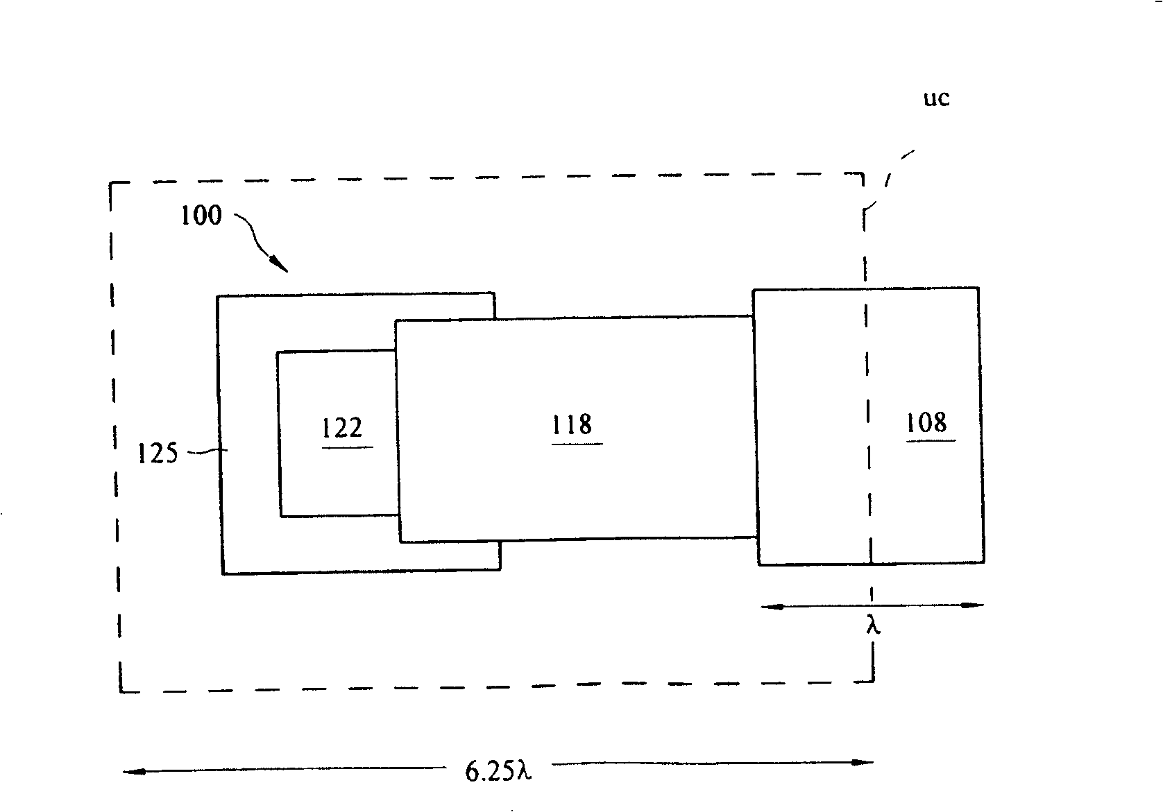
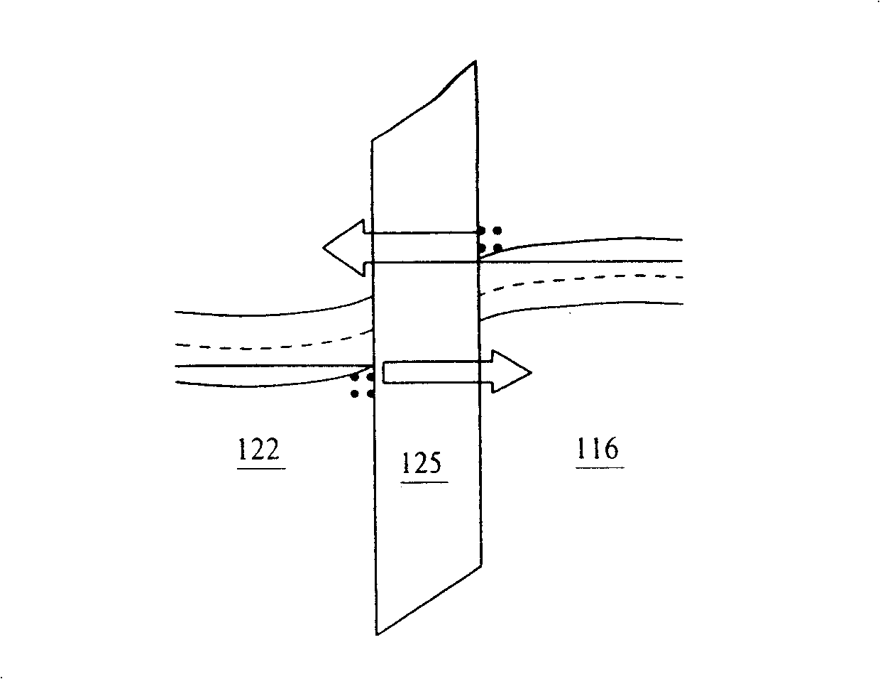
[0073] see figure 1Shown is a cross-sectional view of a DRAM unit cell 100 according to the present invention. The DRAM unit cell 100 mainly includes an NMOS switching transistor 102 and a storage region 104. The switching transistor 102 is provided with a doped n-type channel 106 on a p-type substrate 110 (for example, a p-type silicon wafer having a crystallographic orientation) and heavy Doping n + Drain junction 108 . The switch transistor 102 also includes n + The polysilicon gate structure 118 and the gate oxide layer 120, the source of the transistor 110 are disposed in the storage region 104, as described below.

[00...


PUM


Abstract

The present invention provides a memory cell and method for preparation. The memory cell includes a pass-gate transistor and a storage region. The transistor includes a gate and a drain. The storage region includes a trench, which is preferably a Shallow Trench Isolation (STI). A non-insulating structure, e.g., formed of polysilicon or metal, is located in the trench as serves as a capacitor node. The trench is partially defined by a doped sidewall that serves as a source for the transistor. The poly structure and the trench sidewall are separated by a dielectric layer. The write operation involves charge transport to the non-insulating structure by direct tunneling through the dielectric layer. The read operation is assisted by Gate Induced Drain Leakage (GIDL) current generated on the surface of the sidewall. The embodiments of the invention reduce size of the device, increase storage time of the charge and increase compatibility between the standard preparing steps.

Description

technical field [0001] The present invention relates to a memory device, in particular to a memory cell (Dynamic Random Access Memory, DRAM) of a dynamic random access memory and a manufacturing method thereof. Background technique [0002] Dynamic Random Access Memory (DRAM) is a semiconductor memory device widely used to store electronic data. The existing known DRAM mainly includes standard DRAM (Commodity DARM) and embedded DRAM (Embedded DRAM, eDRAM). [0003] Standard DRAM is a separate, independent memory device that communicates with logic components via the system bus. Current standard DRAM developments include the use of area-optimized single-transistor technology, where the memory cell of the DRAM has a transistor (1T) and a capacitor. In the existing conventional DRAM technology, the capacitance of the single-transistor (1T) memory unit cell is stacked on the transistor (before the formation of the interconnection), or is located in the deep trench (before the ...

Claims


Application Information

Patent Timeline
Patent Type & Authority Patents(China)
IPC IPC(8): H01L27/108H01L21/8242
CPCH01L27/10805H01L27/1085H01L27/10829H10B12/30H10B12/37H10B12/03
Inventor 季明华江文铨陈政谷
Owner TAIWAN SEMICON MFG CO LTD
Why Eureka
Try Eureka