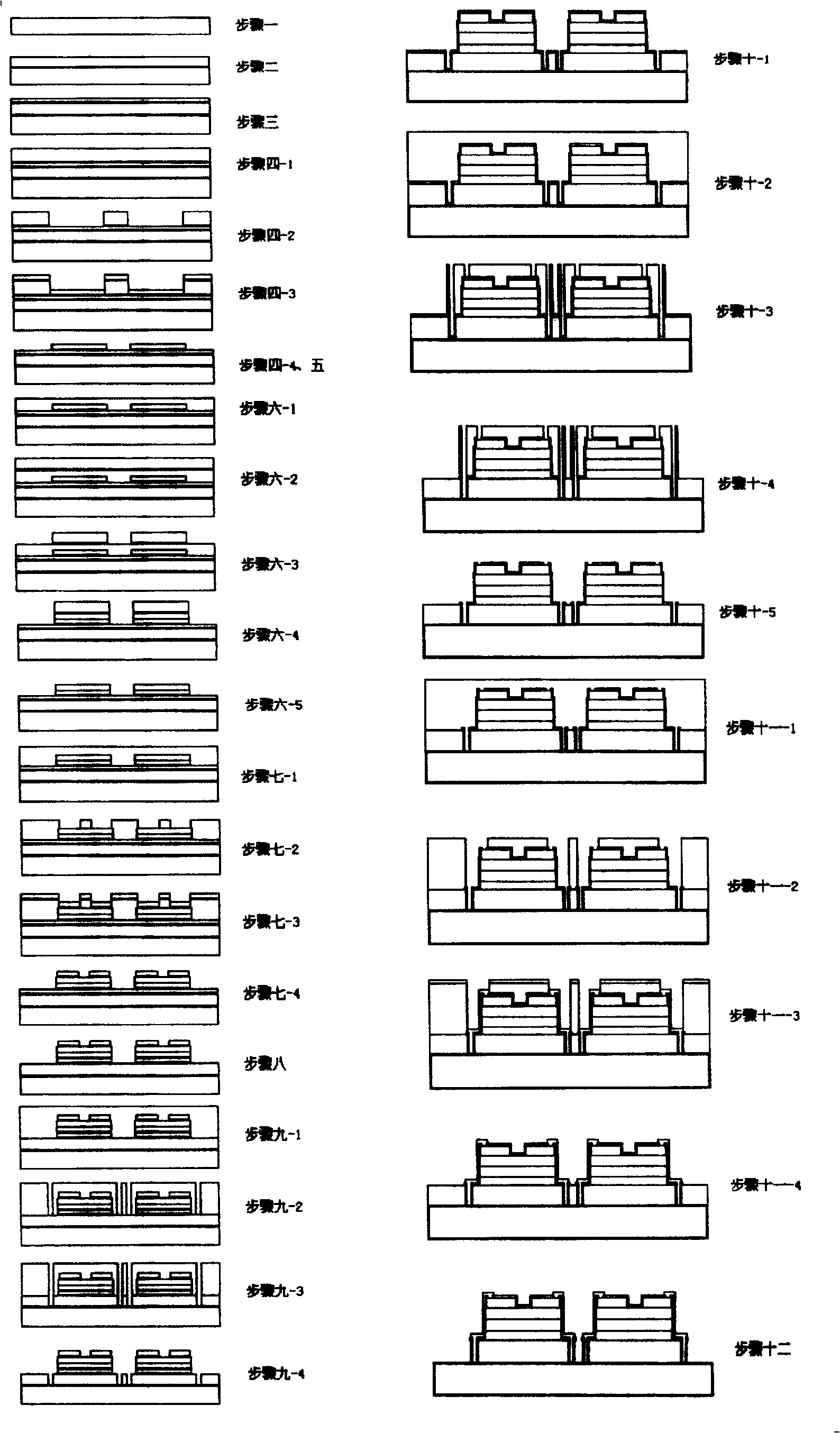
Method for producing lead zirconate-titanate thin film infrared thermal imaging detector hanging structure
A technology of infrared thermal imaging and lead zirconate titanate, which is applied in the field of production, can solve the problems that have not been found in reports or literature, and achieve the effect of good compatibility and simple removal method
- Summary
- Abstract
- Description
- Claims
- Application Information
AI Technical Summary
Problems solved by technology
Method used
Image
Examples
Embodiment 1
[0036] Embodiment 1: The present invention is a method for manufacturing a lead zirconate titanate thin film infrared thermal imaging detector suspension structure. A magnesium oxide film with a certain thickness is plated on a silicon wafer as an uncooled focal plane for making a lead zirconate titanate thin film The sacrificial layer of the suspension structure of the infrared thermal imaging detector, and the suspension height is controlled by controlling the thickness of the sacrificial layer; SiN is fabricated by plasma enhanced chemical vapor deposition (PECVD) x , used to balance the stress of the lead zirconate titanate film; the rapid heat treatment method is applied to the common electrode Ti / Pt and the lead zirconate titanate sensitive film to obtain a high-performance lead zirconate titanate film,
[0037] As shown in Figure 1, the specific steps are as follows:
[0038] Step 1. Use RCA process to clean the single-sided polished silicon substrate, take it out and b...
Embodiment 2
[0052] Process conditions, manufacturing steps, and equipment used are all the same as in Example 1, and the difference is that in step two, the thickness of the plated magnesium oxide film is 1.5 μm; in step three, SiNx The thickness of the film is controlled to be 150nm; in step 6, a PZT film is prepared by a sol-gel method, and the thickness of the film layer is 200nm.
Embodiment 3
[0053] Embodiment 3: process conditions, manufacturing steps, equipment used are all the same as embodiment 1, the difference is: in step two, the thickness of the magnesium oxide film layer is 2.5 μm; in step three, SiN x The thickness of the film is controlled to be 300nm; in step 6, the PZT film is prepared by the sol-gel method, and the thickness of the film layer is 400nm.
PUM
 Abstract
Description
Claims
Application Information


