An asymmetric Schottky barrier MOS transistor and its manufacture method

A MOS transistor and Schottky potential technology, applied in the field of asymmetric Schottky barrier MOS transistors and their fabrication, can solve the problems of small on-state current, large off-state leakage, difficult integrated circuit applications, etc., and reduce complexity. performance, and the effect of reducing off-state leakage current

Inactive Publication Date: 2008-12-31
PEKING UNIV
View PDF4 Cites 2 Cited by
  • Summary
  • Abstract
  • Description
  • Claims
  • Application Information

AI Technical Summary

Problems solved by technology

However, the current research on SBSD MOSFETs has found that due to the existence of the Schottky barrier, the on-state current of the device is small, and the off-state leakage of the Schottky barrier is large, so that the on-off current ratio of the device is not high.
Some researchers have proposed the use of source-drain asymmetric Schottky barriers, which can improve the on-off current ratio of Schottky devices, but the process is not self-aligned, and it is difficult to manufacture in sub-50nm integrated circuits. get applied

Method used


Image

  • An asymmetric Schottky barrier MOS transistor and its manufacture method
  • An asymmetric Schottky barrier MOS transistor and its manufacture method
  • An asymmetric Schottky barrier MOS transistor and its manufacture method

Examples


Embodiment Construction

[0045] The following specific examples help to understand the characteristics and advantages of the present invention, but the implementation of the present invention is by no means limited to the described examples.

[0046] A specific embodiment of the manufacturing method of the present invention includes Figure 1 to Figure 8 Process steps shown:

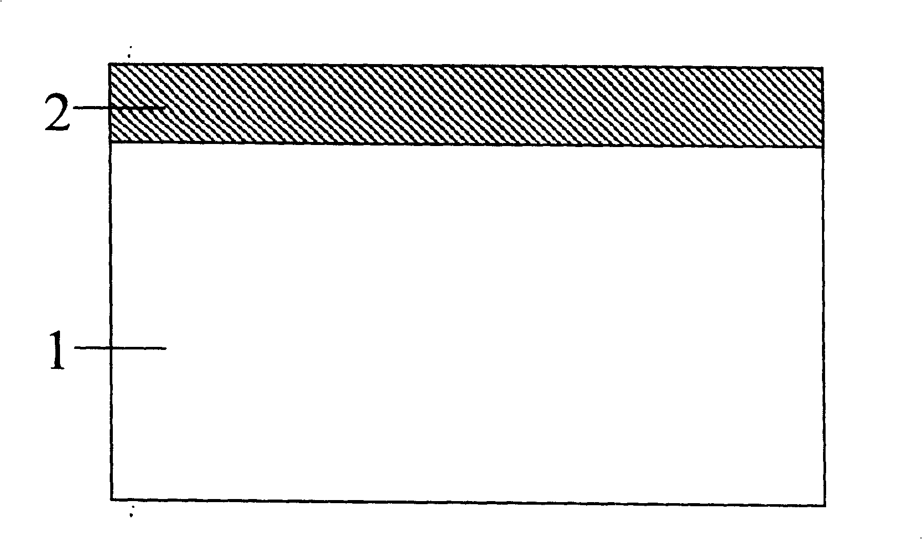
[0047] 1. If figure 1 As shown, the crystal orientation of the bulk silicon wafer silicon substrate (1) used is (100), the body region is initially lightly doped, and the active region isolation layer is fabricated on the substrate by using conventional CMOS shallow trench isolation technology; A layer of TEOS dielectric protection layer (2) is deposited with a thickness of 50-100 nm.

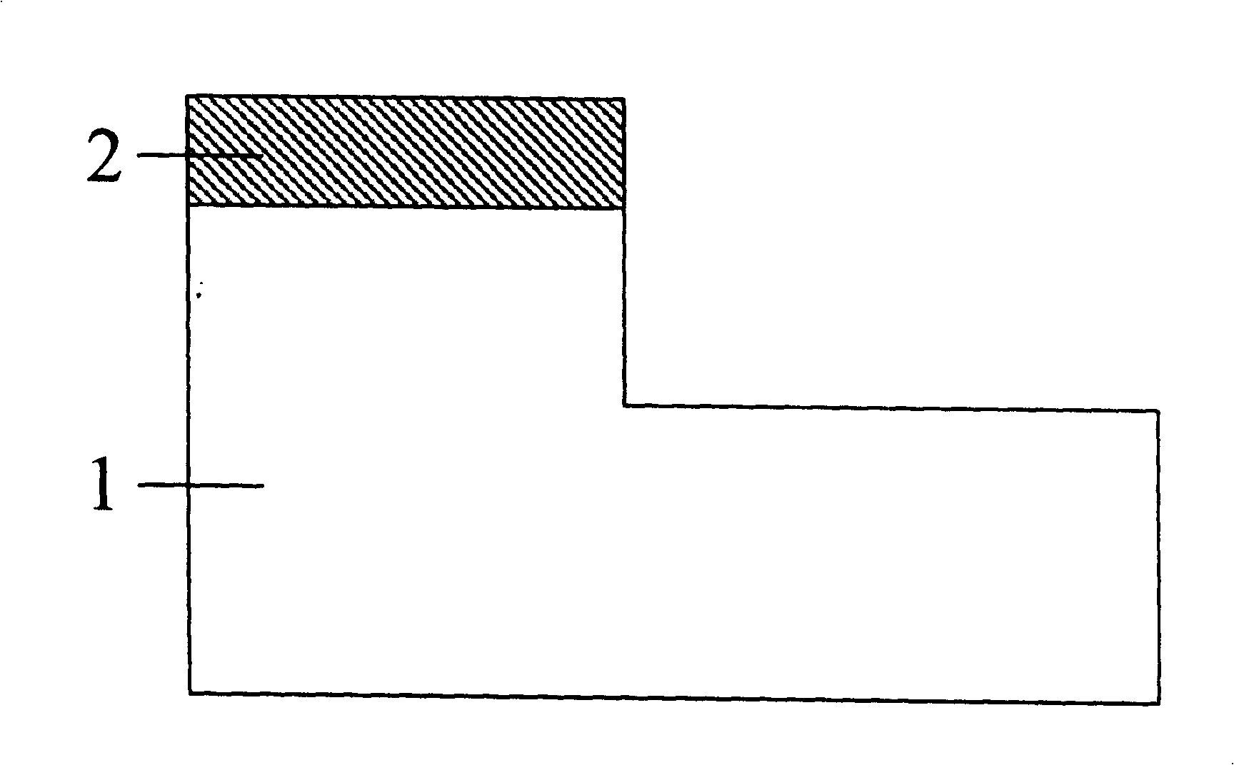
[0048] 2. If figure 2 As shown, photolithography is performed once to etch the TEOS dielectric protection layer (2), and then the unprotected silicon layer is etched to form a step structure, and the etching depth is 10-100nm.
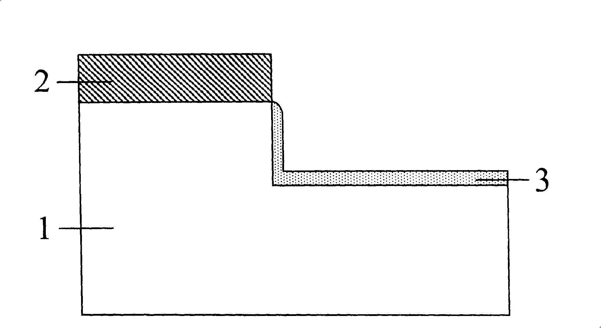
[0049] 3. If...


PUM


Abstract

The provided manufacture method for Schottky barrier source / drain MOS transistor comprises: selecting two types of metal material to prepare asymmetric source and drain; using two metal silicatization reactions, controlling reaction time to obtain the source and drain with different height of Schottky barrier. Compared with prior art, this invention can obtain large on-off current rate or on-state current, while reduces technique complexity, and will fit to sub-50nm scale IC production.

Description

Technical field: [0001] The invention belongs to the technical field of semiconductor integrated circuits and its manufacture, and in particular relates to an asymmetric Schottky barrier MOS transistor and a manufacturing method thereof. Background technique: [0002] Schottky Barrier Source Drain MOSFET (SBSDMOSFET) is a new structure device that is expected to be used in the production of sub-50nm scale integrated circuits. As the feature size of MOSFET devices continues to scale down, traditional MOSFETs encounter a series of insurmountable problems at sub-50nm, such as source-drain parasitic resistance is difficult to scale down, and gate leakage current is too large. Compared with the traditional MOSFET, SBSD MOSFET uses metal and metal silicide instead of highly doped silicon for its source and drain, which greatly improves the device's process complexity and compatibility with new materials. However, the current research on SBSD MOSFETs has found that due to the exis...

Claims


Application Information

Patent Timeline
Patent Type & Authority Patents(China)
IPC IPC(8): H01L29/78H01L29/47H01L21/336H01L21/28
Inventor 孙雷李定宇张盛东吴涛韩汝琦刘晓彦
Owner PEKING UNIV
Why Eureka
Try Eureka