Double medium SOI pressure resistant structure with window and its SOI power device
A power device, dual-dielectric technology, applied in the direction of electric solid state devices, semiconductor devices, electrical components, etc., can solve the problems of difficult process, low breakdown voltage and self-heating effect.
- Summary
- Abstract
- Description
- Claims
- Application Information
AI Technical Summary
Problems solved by technology
Method used
Image
Examples
Embodiment 1
[0052] Embodiment 1: SOI structure with double dielectric buried layer
[0053] Figure 5 It is a schematic diagram of the SOI structure with double dielectric buried layers according to the present invention.
[0054] Such as Figure 5 As shown, 1 is the substrate layer, 2 is the first dielectric layer (buried layer), 3 is the active semiconductor layer (S layer), 14 is the second dielectric layer (buried layer), and 15 is the intermediate layer. The intermediate layer 15 is located between the first dielectric layer (buried layer) 2 and the second dielectric layer (buried layer) 14, the other side of the first dielectric layer is connected to the active semiconductor layer 3, and the other side of the second dielectric layer 14 is connected to the The substrate layer 1 is connected. The first dielectric layer has a window which can be filled with intermediate layer material or active layer material.
Embodiment 2
[0055] Embodiment 2: SOI LDMOS device structure with double dielectric buried layer
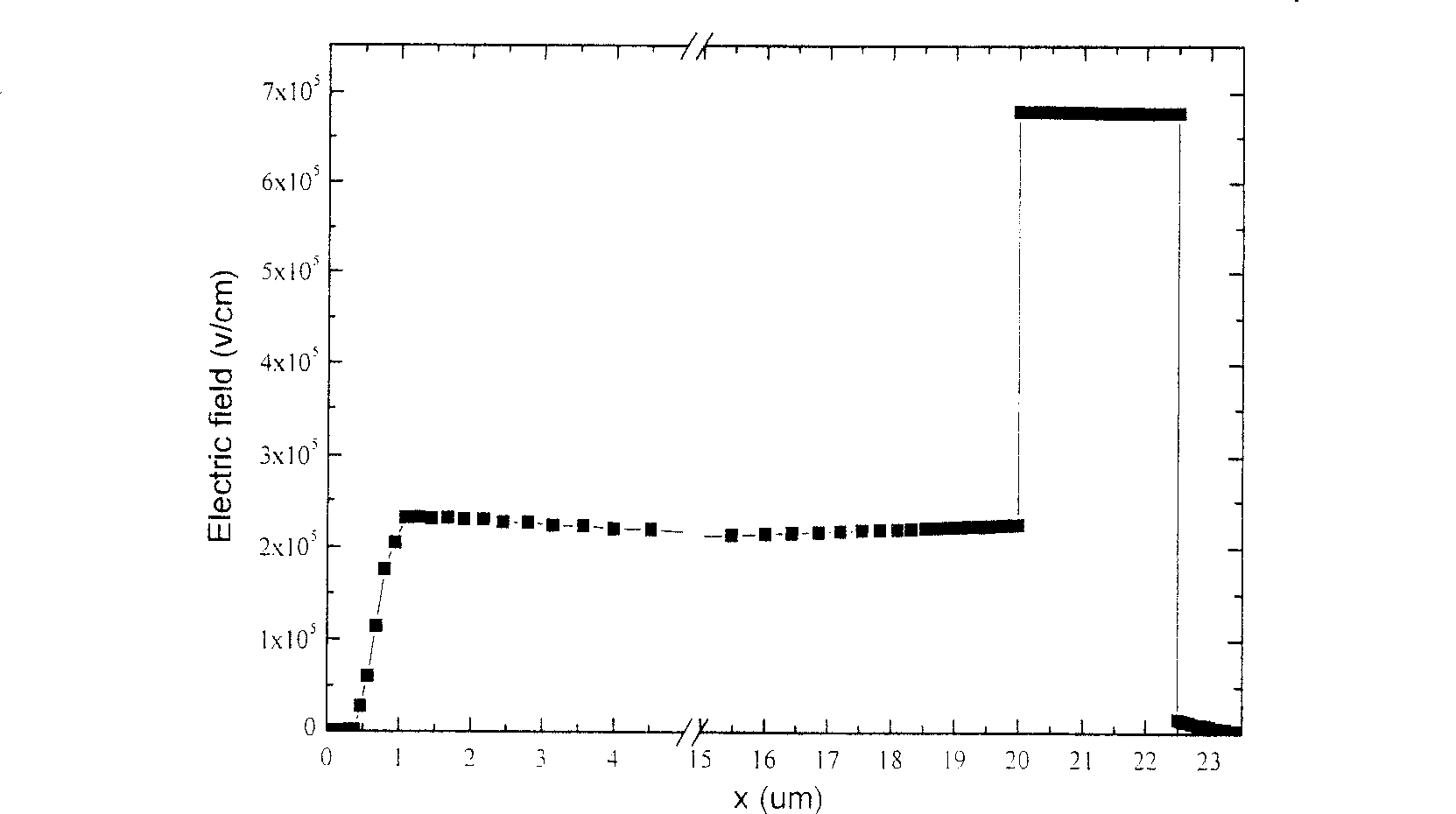
[0056] Image 6 It is a structural schematic diagram of the SOI LDMOS device with double dielectric buried layers according to the present invention, Figure 7 It is a longitudinal electric field distribution diagram of the SOI LDMOS device with double dielectric buried layers according to the present invention. Figure 8 a is a two-dimensional equipotential diagram of a conventional structure SOI LDMOS device when it breaks down. Figure 8 b is a two-dimensional equipotential diagram at the time of breakdown of the SOI LDMOS device with double dielectric buried layers according to the present invention.
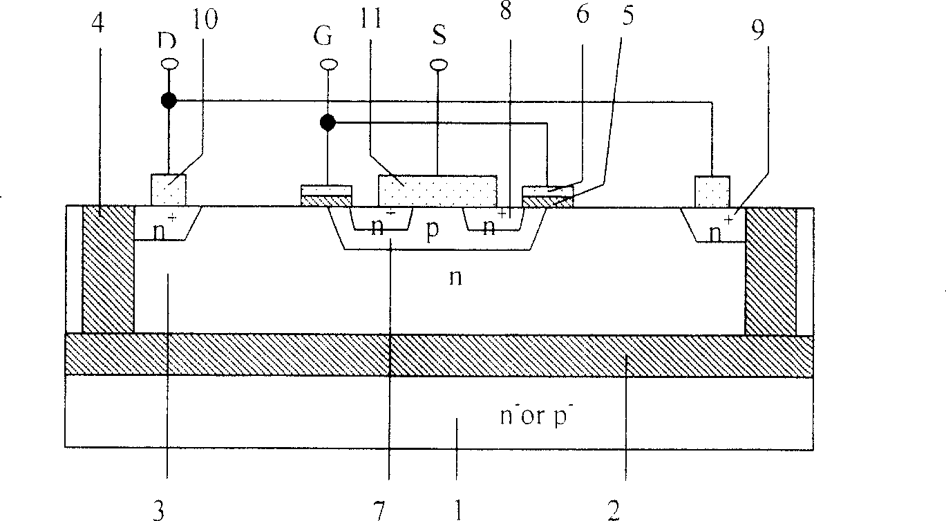
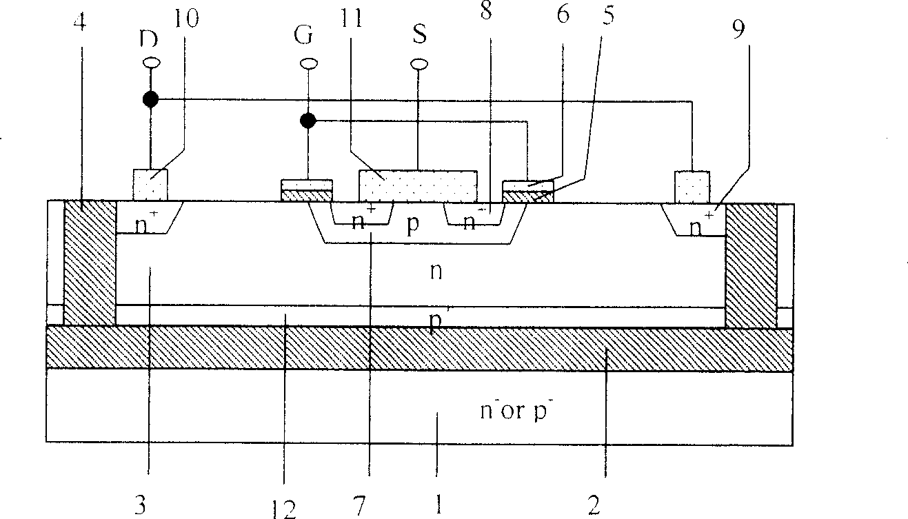
[0057]Such as Image 6 -shown in 8, 1 is the substrate layer, 2 is the first dielectric layer (buried layer), 3 is the active semiconductor layer (S layer), 4 is the dielectric isolation region, 5 is the gate oxide layer, 6 is the gate electrode, 7 For p (or n) well, 8 for n + (or p +...
Embodiment 3
[0058] Embodiment 3: SOI IGBT device structure with double dielectric buried layer
[0059] Figure 9 It is a structural schematic diagram of the SOI IGBT device with double dielectric buried layers according to the present invention.
[0060] Such as Figure 9 As shown, 1 is the substrate layer, 2 is the first dielectric layer, 3 is the active semiconductor layer (S layer), 6 is the gate electrode, 7 is the p (or n) well, and 8 is the n + (or p + ) cathode area, 9 is n + (or p + ) anode region, 14 is the second dielectric layer (buried layer), 15 is the intermediate layer, 17 is the anode, 18 is the cathode, and 19 is the p (or n) well. The intermediate layer 15 is located between the first dielectric layer (buried layer) 2 and the second dielectric layer (buried layer) 14 . The other side of the first dielectric layer is connected to the active semiconductor layer 3 , and the other side of the second dielectric layer 14 is connected to the substrate layer 1 . The firs...
PUM
 Abstract
Description
Claims
Application Information


