

Epitaxial structure of the compound insulation layer nitride high-electronic transfer transistor and its making method
A technology with high electron mobility and composite isolation layer, which is applied in semiconductor/solid-state device manufacturing, circuits, electrical components, etc., can solve the problems of low electron speed and difficulty in improving frequency characteristics, so as to improve frequency characteristics and reduce alloy scattering , The effect of reducing the difficulty of the process
- Summary
- Abstract
- Description
- Claims
- Application Information
AI Technical Summary
Problems solved by technology
Method used
Image

Examples
example 1
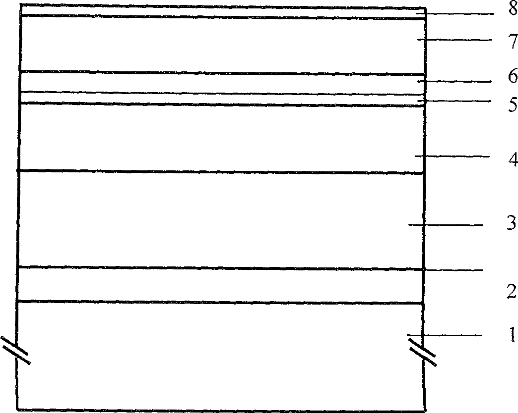
[0044] 1) Select a sapphire substrate, and use the MOCVD method to bake the substrate at 1100°C (or any temperature value between 1000 and 1200°C) in a hydrogen atmosphere for about 10 minutes;
[0045]2) Cool down to 550°C, 500Torr, pass through ammonia gas to nitride the surface for 2 minutes; then pass through ammonia gas and trimethylgallium to grow a 30nm GaN nucleation layer 2; then raise the temperature to 1040°C (can also be controlled any temperature value between 1000~1100℃);
[0046] 3) growing a 2-3 μm high-resistance GaN buffer layer 3 at 1040°C (can also be controlled at any temperature value between 1000-1100°C) and 130 Torr;
[0047] 4) 1040°C (can also be controlled at any temperature value between 1000-1100°C), 200Torr, grow 50nm GaN channel layer 4, according to needs, the thickness of the channel layer 4 can be between 3-200nm select between;
[0048] 5) 1040°C (can also be controlled at any temperature value between 1000-1100°C), 130Torr, grow a 0.8nm Al...
example 2
[0053] 1) Select a silicon carbide substrate, and use MOCVD method to bake the substrate at 1100°C (or any temperature value between 1000 and 1200°C) in a hydrogen atmosphere for 10 minutes;
[0054] 2) Cool down to 1040°C (can also be controlled at any temperature value between 1000-1100°C), feed ammonia and trimethylaluminum to grow a 60nm AlN nucleation layer;
[0055] 3) At 1040°C (can also be controlled at any temperature value between 1000-1100°C), feed ammonia gas and trimethylaluminum to grow a 0.5μm AlN buffer layer;
[0056] 4) 1040°C (can also be controlled at any temperature value between 1000-1100°C), 200Torr, grow 40nm GaN channel layer 4, the thickness of the channel layer 4 can be selected between 3-200nm during specific implementation ;
[0057] 5) 1040°C (can also be controlled at any temperature value between 1000-1100°C), 130Torr, sequentially grow 1.2nm AlN isolation layer 5 and 5nm GaN isolation layer 6, and the thickness of isolation layer 5 can be 0.8-...
example 3
[0062] 1) Select the silicon substrate, after cleaning, use MOCVD method to bake the substrate at 1100°C (or any temperature value between 1000-1200°C) in a hydrogen atmosphere for 10 minutes;
[0063] 2) Cool down to 1050°C (it can also be controlled at any temperature between 1000-1100°C), and trimethylaluminum is passed into the reaction chamber for 60 seconds;
[0064] 3) Passing ammonia gas and trimethylaluminum to grow an 80nm AlN nucleation layer;
[0065] 4) Infuse ammonia gas and trimethylgallium to grow a 1.0 μm GaN high-resistivity buffer layer;
[0066] 5) 200 Torr, growing a 40nm GaN channel layer 4, the thickness of the channel layer 4 can be selected between 3-200nm during specific implementation;
[0067] 6) 1040°C, 150 Torr, sequentially grow 1nm AlN isolation layer 5 and 5nm GaN isolation layer 6, the thickness of isolation layer 5 can be selected between 0.8nm and 2nm, and the thickness of isolation layer 6 can be between 1nm and 6nm. select;
[0068] 7) ...
PUM
 Abstract
Description
Claims
Application Information