

Continuous-surface shape mask moving photoetching exposure device
An exposure device and mask technology, which is applied in microlithography exposure equipment, photolithography exposure device, optics, etc., can solve the problem that the quality and production efficiency of continuous surface components cannot be greatly improved, the continuous surface shape of components is not smooth enough, Insufficient production function, production precision, operation and convenience, etc., to achieve the effect of continuous distribution of exposure dose, complete functions, and cheap equipment
- Summary
- Abstract
- Description
- Claims
- Application Information
AI Technical Summary
Problems solved by technology
Method used
Image

Examples
Embodiment Construction
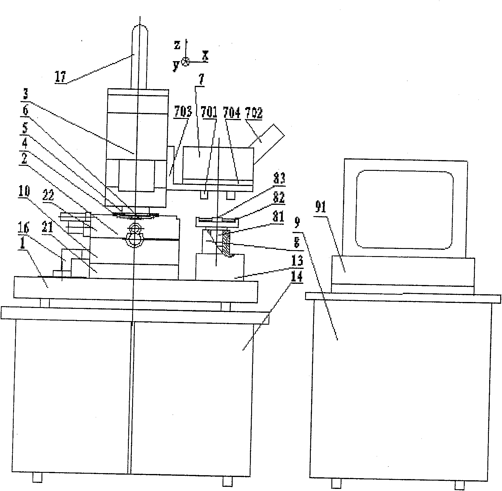
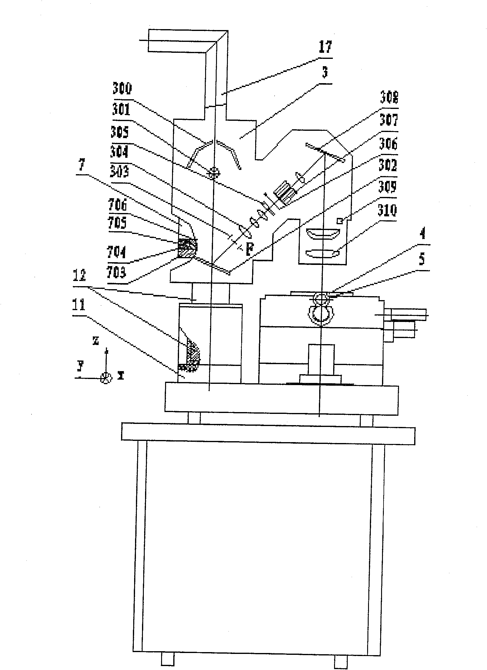
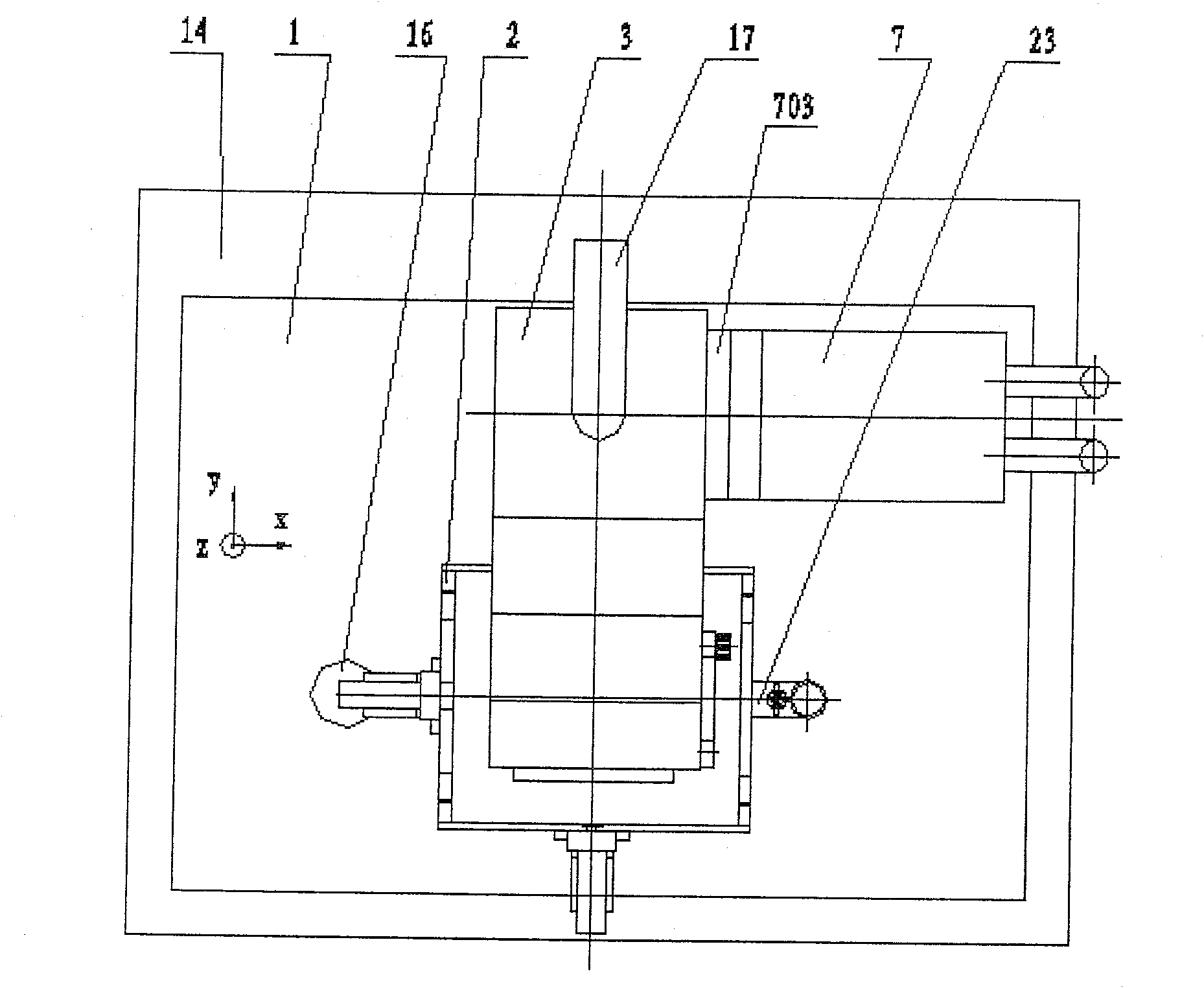
[0024] Such as figure 1 As shown, the present invention includes a host large substrate 1, a mask moving table system 2, a uniform illumination system 3, a mask frame 4, a mask 5, a substrate 6, an alignment observation system 7, an illumination uniformity detection system 8 and The control system 9 and the large base plate 1 of the main machine are placed on the vibration isolation platform 14 composed of air feet, so that the main machine of the present invention is not affected by the vibration of the external environment when performing the photolithography exposure of the moving mask. On the large substrate 1 of the host machine, a mask mobile workbench system 2 and an illumination uniformity detection system 8 are respectively fixed, wherein the illumination uniformity detection system 8 is connected to the large substrate 1 through a bracket 13, and the mask mobile workbench system 2 is located on the ground floor The XY manual table 21 and the XY mask moving table 22 c...
PUM
| Property | Measurement | Unit |
|---|---|---|
| surface roughness | aaaaa | aaaaa |
Abstract
Description
Claims
Application Information