A method for making CDSEM calibration sample

A production method and sample technology, applied in semiconductor/solid-state device manufacturing, electrical components, semiconductor/solid-state device testing/measurement, etc., can solve problems such as short service time, drift of measured values, inaccurate measured values, etc., and achieve work The effect of life extension

Inactive Publication Date: 2007-08-01
SEMICON MFG INT (SHANGHAI) CORP +1
View PDF0 Cites 13 Cited by
  • Summary
  • Abstract
  • Description
  • Claims
  • Application Information

AI Technical Summary

Problems solved by technology

It is chosen to measure the performance of the reaction machine, but the problem often encountered in the application is: when the measured standard sample wafer is exposed to the electron beam of the scanning electron microscope (SEM), its CD will produce "growth". "(grow) phenomenon
Charge-induced hydrocarbon contamination causes measurement drift that makes it impossible to match line/s...

Method used


Image

  • A method for making CDSEM calibration sample
  • A method for making CDSEM calibration sample

Examples


Embodiment Construction

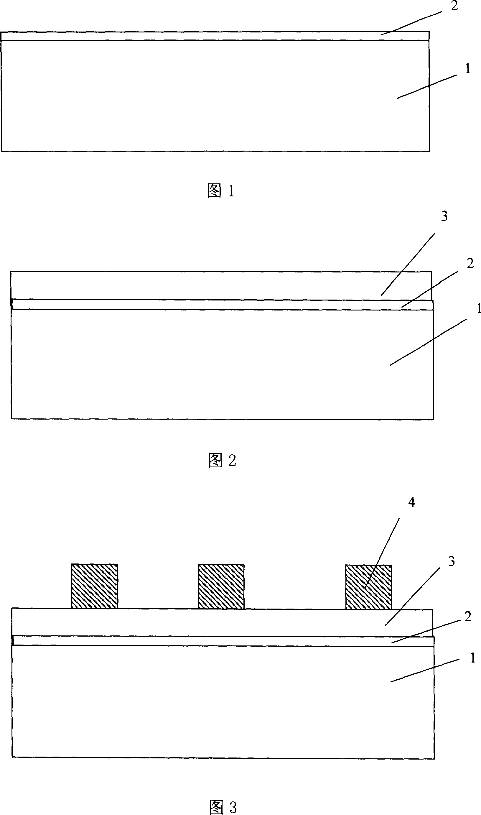
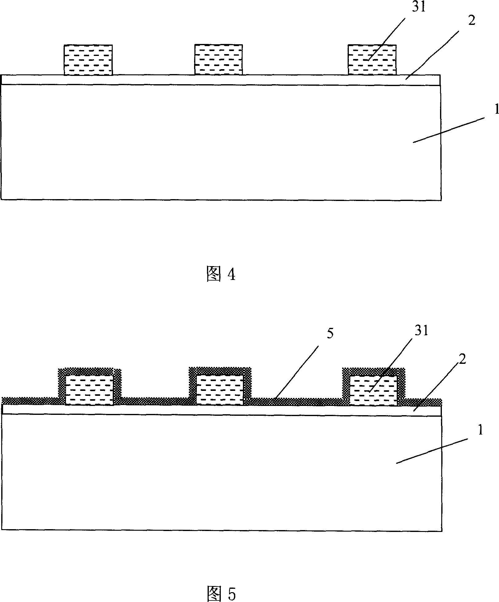
[0033] A kind of equipment of the present invention measures key dimension in semiconductor manufacturing process, as the preparation method of the sample that CDSEM carries out calibration, comprises:

[0034] Fabrication of the polysilicon gate structure and forming a conductive layer on the entire surface of the polysilicon gate structure.

[0035] The polysilicon grid structure of the present invention can be made according to the fabrication method of the conventional polysilicon grid structure, that is, at first pre-cleaning is carried out on the silicon substrate, and sulfuric acid (H 2 SO 4 ), hydrofluoric acid (HF), ammonia + hydrogen peroxide + deionized water (NH 4 OH+H 2 o 2 +DI), hydrochloric acid + hydrogen peroxide + deionized water (HCL+H 2 o 2 +DI) to remove oxides or pollutants on the surface of the wafer; then thermal oxidation and other methods are used to form a pad oxide layer, generally at a temperature of 900-1100°C to form an oxide layer with a th...


PUM

PropertyMeasurementUnit
Thicknessaaaaaaaaaa
Thicknessaaaaaaaaaa
Thicknessaaaaaaaaaa

Abstract

A manufacturing method of measuring key size of scanning electronic microscope (CDSEM) calibration sample includes pre-cleanout of silicon underlay, forming underlay oxidizing layer, accumulating multi crystal silicon layer, forming photosensitive resist pattern, forming gate structure, forming a conducting layer. Gate structure sample gained restrains the aggradation of hydrocarbon induced by cumulation of surface charge for the abreaction effect of conducting layer, so the phenomenon of overloading of CD grown is eliminated to make service life of the calibration sample prolong apparently and guarantee the reliability of test of CDSEM.

Description

technical field [0001] The invention relates to the calibration of equipment in the semiconductor manufacturing process, in particular to a sample used for calibrating a critical dimension scanning electronic microscope (Critical Dimension Scanning Electronic Microscope, CDSEM) in the semiconductor manufacturing process and a manufacturing method thereof. Background technique [0002] A critical dimension scanning electron microscope (hereinafter referred to as CDSEM) is an instrument used to measure the critical dimension (hereinafter referred to as CD) of a pattern formed on a wafer in a semiconductor manufacturing process. CDSEM needs to be calibrated with specific standard samples so that the measurements of the individual instruments are matched and consistent. [0003] In the manufacturing process of semiconductor devices, the polysilicon gate is the most important process, and its critical dimension CD is also the smallest. Therefore, polysilicon gate (Poly Gate) stru...

Claims


Application Information

Patent Timeline
IPC IPC(8): H01L21/66H01L21/336
Inventor 严博薛玢杨欣郭力奇
Owner SEMICON MFG INT (SHANGHAI) CORP
Why Eureka
Try Eureka