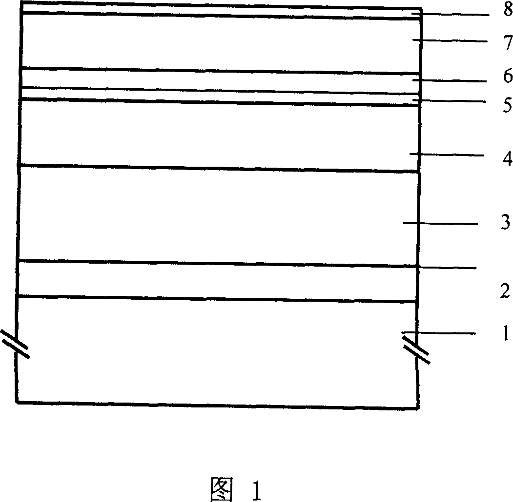
Epitaxial structure of the compound insulation layer nitride high-electronic transfer transistor and its making method
A high electron mobility, composite isolation layer technology, applied in semiconductor/solid-state device manufacturing, circuits, electrical components, etc., can solve the problems of low electron speed and difficult to improve frequency characteristics, to improve frequency characteristics and reduce alloy scattering , The effect of reducing the difficulty of the process
- Summary
- Abstract
- Description
- Claims
- Application Information
AI Technical Summary
Problems solved by technology
Method used
Image
Examples
example 1
[0044] 1) Select a sapphire substrate, and use the MOCVD method to bake the substrate at 1100°C (or any temperature value between 1000 and 1200°C) in a hydrogen atmosphere for about 10 minutes;
[0045]2) Cool down to 550°C, 500Torr, pass through ammonia gas to nitride the surface for 2 minutes; then pass through ammonia gas and trimethylgallium to grow a 30nm GaN nucleation layer 2; then raise the temperature to 1040°C (can also be controlled any temperature value between 1000~1100℃);
[0046] 3) growing a 2-3 μm high-resistance GaN buffer layer 3 at 1040°C (can also be controlled at any temperature value between 1000-1100°C) and 130 Torr;
[0047] 4) 1040°C (can also be controlled at any temperature value between 1000-1100°C), 200Torr, grow 50nm GaN channel layer 4, according to needs, the thickness of the channel layer 4 can be between 3-200nm select between;
[0048] 5) 1040°C (can also be controlled at any temperature value between 1000-1100°C), 130Torr, grow a 0.8nm Al...
example 2
[0053] 1) Select a silicon carbide substrate, and use MOCVD method to bake the substrate at 1100°C (or any temperature value between 1000 and 1200°C) in a hydrogen atmosphere for 10 minutes;
[0054] 2) Cool down to 1040°C (can also be controlled at any temperature value between 1000-1100°C), feed ammonia and trimethylaluminum to grow a 60nm AlN nucleation layer;
[0055] 3) At 1040°C (can also be controlled at any temperature value between 1000-1100°C), feed ammonia gas and trimethylaluminum to grow a 0.5μm AlN buffer layer;
[0056] 4) 1040°C (can also be controlled at any temperature value between 1000-1100°C), 200Torr, grow 40nm GaN channel layer 4, the thickness of the channel layer 4 can be selected between 3-200nm during specific implementation ;
[0057] 5) 1040°C (can also be controlled at any temperature value between 1000-1100°C), 130Torr, sequentially grow 1.2nm AlN isolation layer 5 and 5nm GaN isolation layer 6, and the thickness of isolation layer 5 can be 0.8-...
example 3
[0062] 1) Select the silicon substrate, after cleaning, use MOCVD method to bake the substrate at 1100°C (or any temperature value between 1000-1200°C) in a hydrogen atmosphere for 10 minutes;
[0063] 2) Cool down to 1050°C (it can also be controlled at any temperature between 1000-1100°C), and trimethylaluminum is passed into the reaction chamber for 60 seconds;
[0064] 3) Passing ammonia gas and trimethylaluminum to grow an 80nm AlN nucleation layer;
[0065] 4) Infuse ammonia gas and trimethylgallium to grow a 1.0 μm GaN high-resistivity buffer layer;
[0066] 5) 200 Torr, growing a 40nm GaN channel layer 4, the thickness of the channel layer 4 can be selected between 3-200nm during specific implementation;
[0067] 6) 1040°C, 150 Torr, sequentially grow 1nm AlN isolation layer 5 and 5nm GaN isolation layer 6, the thickness of isolation layer 5 can be selected between 0.8nm and 2nm, and the thickness of isolation layer 6 can be between 1nm and 6nm. select;
[0068] 7) ...
PUM
 Abstract
Description
Claims
Application Information
 - R&D
- Intellectual Property
- Life Sciences
- Materials
- Tech Scout
- Unparalleled Data Quality
- Higher Quality Content
- 60% Fewer Hallucinations
Browse by: Latest US Patents, China's latest patents, Technical Efficacy Thesaurus, Application Domain, Technology Topic, Popular Technical Reports.
© 2025 PatSnap. All rights reserved.Legal|Privacy policy|Modern Slavery Act Transparency Statement|Sitemap|About US| Contact US: help@patsnap.com

