

Positive photosensitive resist release agent compositions
A photoresist and stripper technology, applied in the processing of photosensitive materials, etc., can solve the problems of unsatisfactory stripping performance, large resist damage, harsh etching conditions, etc., to achieve excellent solubility and stripping, low temperature Excellent peeling performance and favorable working environment
- Summary
- Abstract
- Description
- Claims
- Application Information
AI Technical Summary
Problems solved by technology
Method used
Image

Examples
Embodiment 1-18 and comparative example 1-10
[0065] According to the ratio described in Table 1 below, the organic amines, organic solvents and polar solvents were formulated to prepare the stripping solution. According to the content of the polar solvent, each release agent was evaluated in terms of peelability, corrosion and evaporation loss, and the evaluation results are shown in Table 2 below.
[0066] [Table 1]
[0067] Composition of stripping agent (wt%)
[0068] Example 7
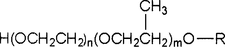
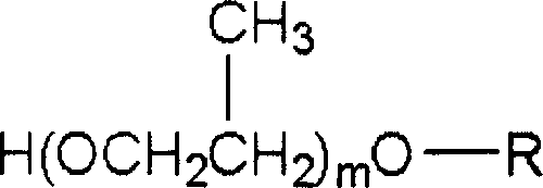
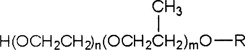
[0069] In Table 1, A: organic amine, B: diethylene glycol monoalkyl ether, C: aprotic polar solvent, D: nonionic surfactant, wherein, examples 1-5 are polyoxypropylene glycol ethers , Examples 6-10 are polyoxypropylene ethyl ethers, examples 11-14 are polyoxyethylene polypropylene glycol ethers, and examples 15-18 are polyoxyethylene polypropylene glycol ethers.
[0070] MEA: Monoethanolamine (Monoethanolamine);
[0071] DEA: diethanolamine (diethanolamine);
[0072] TEA: Triethanolamine (Triethanolamine);
[0073]BD...
PUM
 Abstract
Description
Claims
Application Information