

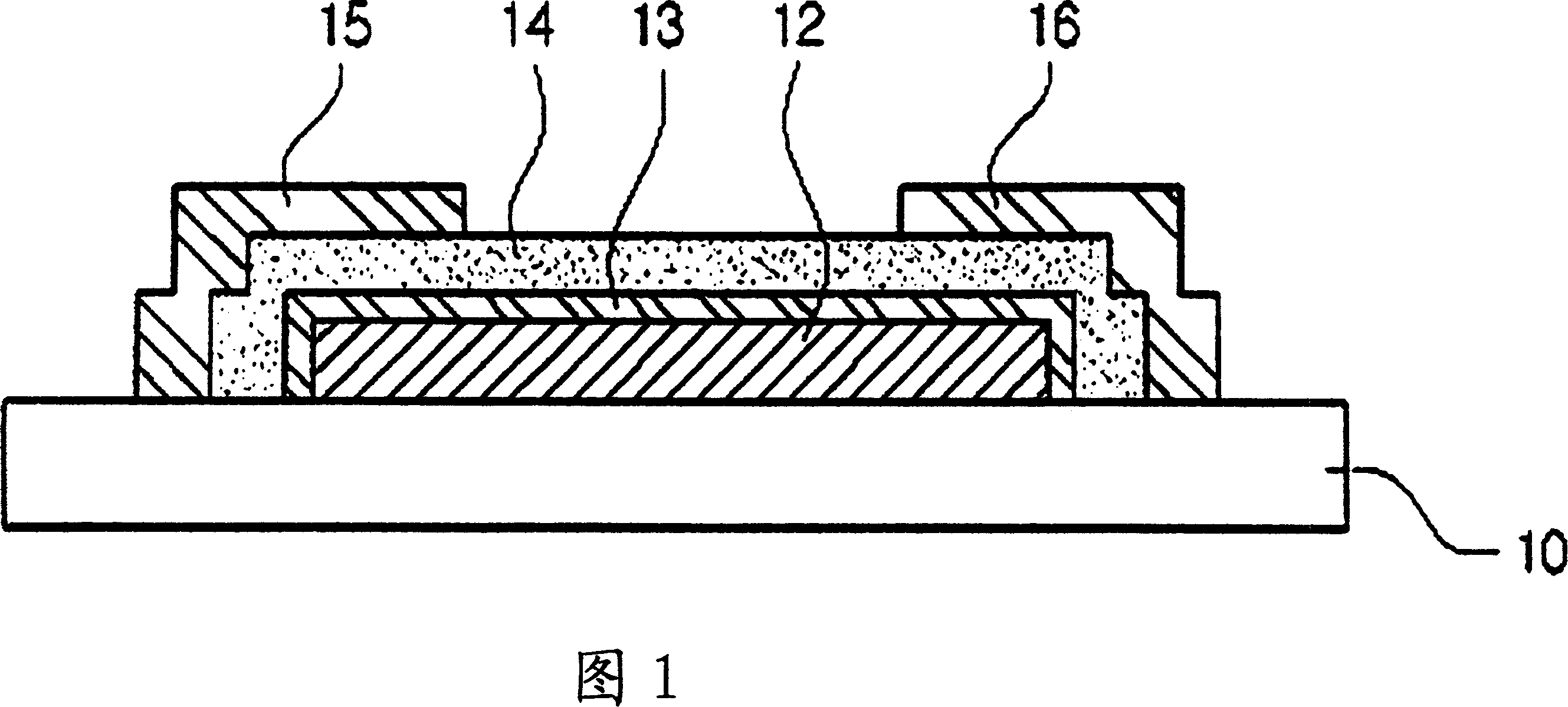
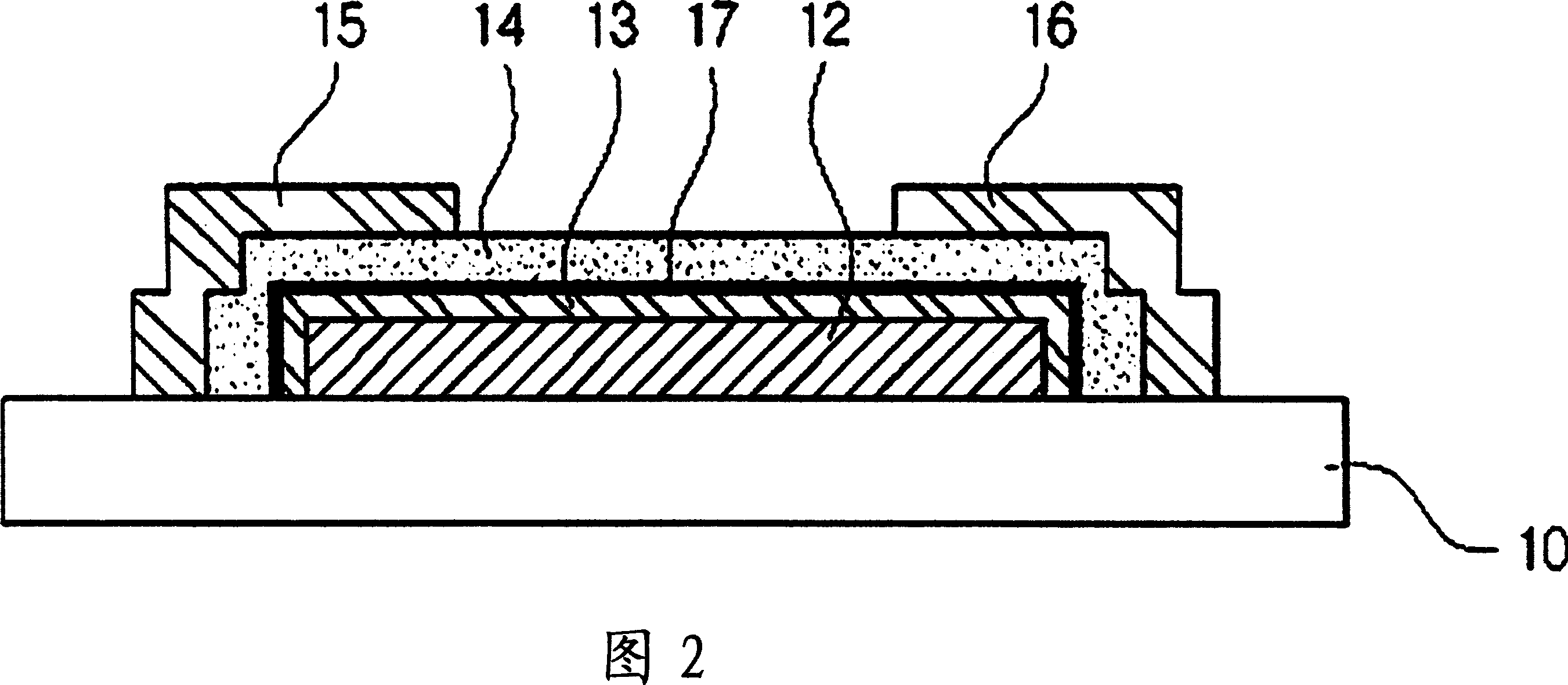
Low-voltage organic thin film transistor and fabrication method thereof
A technology of gate dielectric layer and organic thin film, applied in the field of OTFT, which can solve the problems of unfavorable metal peeling and lack of usability
- Summary
- Abstract
- Description
- Claims
- Application Information
AI Technical Summary
Problems solved by technology
Method used
Image

Examples
experiment example 1
[0034] Experimental Example 1: Electrical Characteristics of Aluminum Oxide
[0035] To determine the electrical properties of the alumina shown in Figure 5, I-V (current-voltage) and C-V (capacitance-voltage) measurements were performed using appropriate instruments, HP4155A and HP4280A, respectively. Figures 6 to 8 obtained from these experiments show the I-V characteristic curve, fault voltage curve, and capacitance curve of the aluminum oxide layer, respectively.
[0036] Figure 6 plots Al / Al 2 o 3 / Al structure and Al / Al 2 o 3 / I-V curves in the Au structure. The results in Figure 6 show different leakage current densities in the two structures. For example, the Al / Al 2 o 3 / Al structure exhibits a relatively high current density of 5.87×10 at 1V -7 A / cm 2 , otherwise the Al / Al 2 o 3 / Au structure has a relatively low current density of 2.4×10 at 1V -7 A / cm 2 . This may be due to the difference in work function between aluminum and gold.
[0037] As shown i...
experiment example 2
[0039] Experimental example 2: Electrical characteristics of pentacene OTFT
[0040] Figure 9A and Figure 9B show the I of the pentacene OTFT with aluminum oxide layer shown in Figure 5 DS -V GS , I DS -V DS characteristic curve. Its electrical characteristics are shown in Table 1 below.
[0041] Table I
[0042] mobility
(cm 2 / V·sec)
ON / OFF current rate
(I on / I off )
subcritical slope
(V / dec)
power off state
Flow (pA / μm)
0.1
6.3×10 3
-1.13
0.206
0.25
[0043] As shown in Table 1, the OTFT has a 0.1cm 2 / V·sec Mobility, 6.3×10 3 The on / off current rate (I on / I off ), -1.13V critical voltage (V t ), a critical slope of 0.206V / dec, and an on-state current of 0.25pA / μm. Furthermore, at V GS =-2V, the drain / source soak voltage (V DS,sat ) was measured as -0.7V, and thus confirms the low voltage operation of the OTFT.
[0044] As fully discussed above, the inventive l...
PUM
 Abstract
Description
Claims
Application Information