Organic electroluminescent device with hybrid illuminating layer

A technology of electroluminescent devices and light-emitting layers, which is applied in the direction of electroluminescent light sources, electric solid-state devices, electrical components, etc., can solve the problems of low luminous efficiency of devices, and achieve the effect of improving luminous efficiency and enhancing brightness efficiency

Inactive Publication Date: 2007-09-05
SOUTHEAST UNIV
View PDF0 Cites 18 Cited by
  • Summary
  • Abstract
  • Description
  • Claims
  • Application Information

AI Technical Summary

Problems solved by technology

In addition, the mobility of holes in NPB is higher than that of electrons in Alq 3 3 It is much higher, therefore, the current generated by holes is much larger than the current generated by electrons, because of the imbalance of hole and electron injection, the device has only low luminous efficiency

Method used


Image

  • Organic electroluminescent device with hybrid illuminating layer
  • Organic electroluminescent device with hybrid illuminating layer
  • Organic electroluminescent device with hybrid illuminating layer

Examples


Embodiment Construction

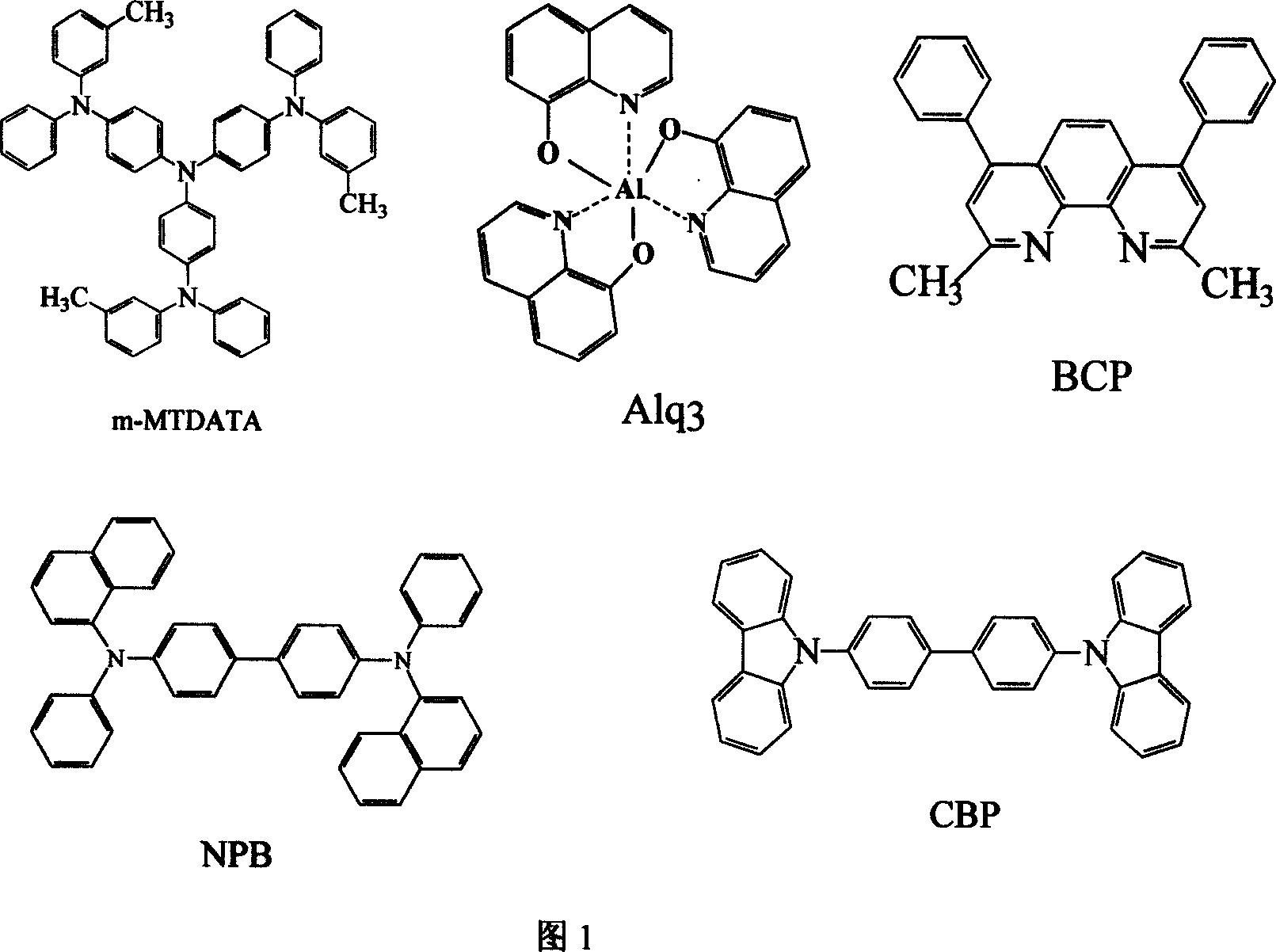
[0049] Figure 1 shows the structure of the organic small molecule material in this study. OLEDs are fabricated on ITO. The thickness of the ITO layer is about 60nm, and its sheet resistance is 50Ω. Conventional cleaning steps include ultrasonic cleaning the ITO layer in acetone, alcohol, isopropanol, and deionized water, and finally irradiating it in an oxygen plasma chamber. After treatment in an oxygen plasma chamber, the ITO substrate was placed in a vacuum chamber for device fabrication. This main vacuum chamber houses ten emission sources, each heated by a tantalum heater, the opening and closing of the baffles controls the deposition sequence, deposition rate and thickness by a quartz oscillator consisting of a crystal sensor and frequency counter device measurement. In order to obtain a large-area uniform film and a steep interface, three types of baffles are installed in the vacuum chamber. For example, in addition to the baffles used for the crucible, there is also...


PUM

PropertyMeasurementUnit
thicknessaaaaaaaaaa
thicknessaaaaaaaaaa
thicknessaaaaaaaaaa

Abstract

The invention is concerned with organic light-emitting devices (OLED) with complexes luminescent layer. It designs and improves the structure of organic light-emitting devices to get high efficiency and capability for the light information display and illumination field. Treat the transparent conductive glass substrate containing indium tin oxide-ITO with six layers materials. The first layer is 4, 4', 4'-tri(N-3-methyl-N- phenyl-amino)triphenylamines, i.e. m-MTDATA with 10 to 100 nm thickness, the second layer is N, N'-di(naphthyl-2-group)-N, N'-diphenylethene-di-diamino biphenyl, i.e. NPB layer with 20 to 100 nm thickness, the third layer is 4, 4'-di(carbazole -9-group)- biphenyl and tri-(8-hydroxy-quinolinato) aluminium, the forth layer is 2,9-dimethyl-4, 7-diphenylethene -1, 110-penanthroline, the fifth layer is tri-(8-hydroxy-quinolinato) aluminium, i.e. Alq3 layer, the sixth layer is alloy of magnesium and silver- Mg:Ag with 100 to 300 nm thickness.

Description

technical field [0001] The present invention is about designing and optimizing the structure of organic light-emitting diodes (OLEDs) to obtain higher efficiency and performance, which can be applied in the field of optical information display and lighting. Background technique [0002] Organic light-emitting diodes, also known as organic light-emitting diodes (OLEDs), have gained in importance in recent years due to their potential for multicolor self-emitting flat panel displays and lighting1,2. The use of organic multilayer structure and doping technology can effectively reduce its driving voltage and increase the performance of the device, which is very important in practical applications. Because the multilayer structure device can balance the injection / transport of holes and electrons, it can confine excitons in the light-emitting layer (LEL) away from the cathode, and it can also reduce the mismatch of energy levels between organic materials and electrodes. In order ...

Claims


Application Information

Patent Timeline
Patent Type & Authority Applications(China)
IPC IPC(8): H01L51/50H01L51/54H05B33/14C09K11/06
Inventor 孙小卫陈佰军徐春祥王保平
Owner SOUTHEAST UNIV
Why Eureka
Try Eureka