Manufacturing method for array substrate of thin film transistor LCD

A technology of thin film transistors and array substrates, which is applied in the production field of array substrates of thin film transistor liquid crystal displays, can solve the problems of high cost and low yield rate, and achieve the effects of simplifying the manufacturing process, improving production efficiency, improving efficiency and reliability

Active Publication Date: 2007-09-12
BEIJING BOE OPTOELECTRONCIS TECH CO LTD +1
View PDF0 Cites 45 Cited by
  • Summary
  • Abstract
  • Description
  • Claims
  • Application Information

AI Technical Summary

Problems solved by technology

The above defects have caused disadvantages such as low yield rate and high cost in manufacturing

Method used


Image

  • Manufacturing method for array substrate of thin film transistor LCD
  • Manufacturing method for array substrate of thin film transistor LCD
  • Manufacturing method for array substrate of thin film transistor LCD

Examples


Embodiment Construction

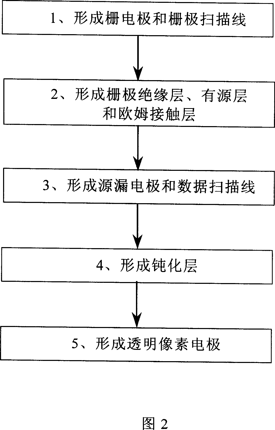
[0037] Below in conjunction with accompanying drawing and specific embodiment, the present invention is described in further detail:

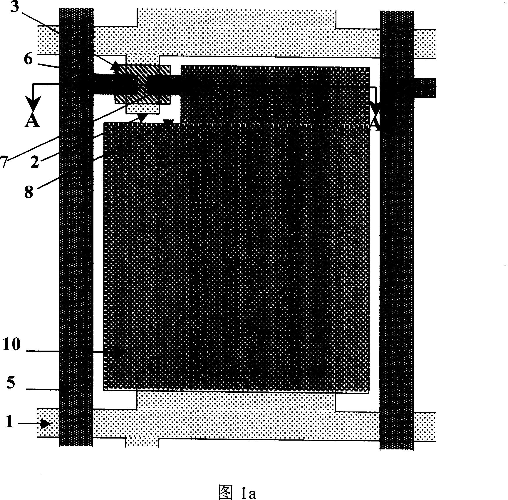
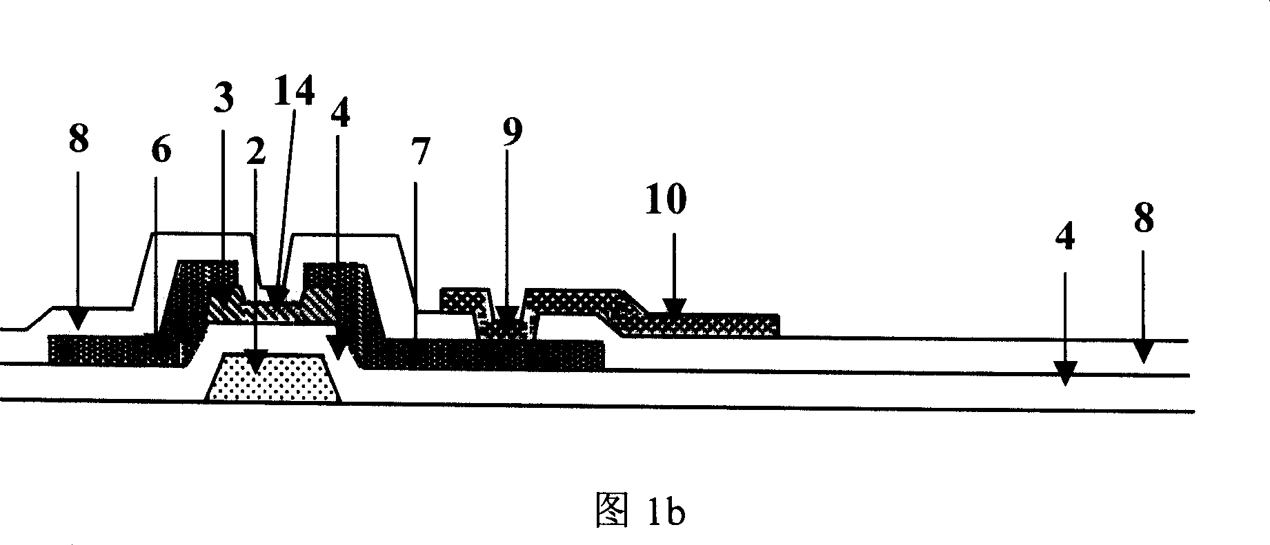
[0038] First, a gate metal thin film with a thickness of 1000 Ȧ to 7000 Ȧ is prepared on the substrate by magnetron sputtering. The gate metal thin film is usually made of metals such as molybdenum, aluminum, aluminum-nickel alloy, molybdenum-tungsten alloy, chromium, or copper, or a combination of the above-mentioned materials. As shown in FIG. 3 a and FIG. 3 b , the first mask plate is used for exposure and development, and then chemical etching is performed to form patterns of gate scanning lines 1 and gate electrodes 2 on a certain area of ​​the glass substrate.

[0039] Then, a gate insulating layer 4 film with a thickness of 1000 Ȧ to 6000 Ȧ and a semiconductor layer 3 film (including an active layer and an ohmic contact layer) with a thickness of 1000 Ȧ to 6000 Ȧ are successively deposited on the array substrate by chemical vapor deposit...


PUM


Abstract

The invention opens a manufacturing method of the thin film transistor liquid crystal display array substrate. Including the following steps: first, forms the first metal film on the substrate; uses the version of the first layer metal film define the design of the first metal film and to form grid scan line and grid electrode. Next, the first insulating layer, the active layer, ohmic contact layer and the second layer metal film were deposited above the metal grid in turn; The use of the second block mask, namely, a gray-first definition of the second mask layer metal film patterns, forms a source of leakage and data scanning lines; Secondly forms the active layer island and conductive thin film transistor device channel. Then it forms the second insulation film on the second metal layer. Finally, the use of the third block mask, that is the second block of gray-definition version of the second mask layer insulation film, forms a second layer insulation film designs, makes some part of the second layer and the second layer of metal insulation layer exposed, and the other part was the protection of light-sensitive materials. Here a transparent conductive film deposits on it, and then removes light sensitive materials and their attachment -the electro-conductive film, finally forms the design of the electric conduction thin film.

Description

technical field [0001] The invention relates to a manufacturing method of an array substrate of a thin film transistor liquid crystal display (TFT-LCD). Background technique [0002] In the thin film transistor liquid crystal display industry, reducing the number of masking processes for array substrates is an effective way to reduce production costs. The traditional array substrate manufacturing process has evolved from six masking processes to five masking processes, and is further simplified to four masking processes. By reducing the number of photolithography processes, the use of materials and production costs can be reduced, and the utilization efficiency and production capacity of existing equipment can also be improved. Currently, the mainstream manufacturing processes in the industry are the five-pass mask process and the four-pass mask process. [0003] 1a and 1b are a top view and a schematic cross-sectional view of a single pixel of a current mainstream thin fi...

Claims


Application Information

Patent Timeline
Patent Type & Authority Applications(China)
IPC IPC(8): G03F7/20G03F7/42H01L21/027G02F1/136
Inventor 龙春平
Owner BEIJING BOE OPTOELECTRONCIS TECH CO LTD
Why Eureka
Try Eureka