Crystal silicon solar battery with multi-hole silicon layer structure

A technology of solar cells and porous silicon layers, applied in the field of solar cells, to achieve the effects of reducing consumption, improving photoelectric conversion efficiency, long life value and diffusion length

Inactive Publication Date: 2007-10-17
SHANGHAI SOLAR ENERGY S&T
View PDF0 Cites 5 Cited by
  • Summary
  • Abstract
  • Description
  • Claims
  • Application Information

AI Technical Summary

Problems solved by technology

[0003] Aiming at the defects existing in the prior art, in order to solve the structural problems of the existing crystalline silicon solar cells, the present invention provides a crystalline silicon solar cell...

Method used


Image

  • Crystal silicon solar battery with multi-hole silicon layer structure
  • Crystal silicon solar battery with multi-hole silicon layer structure

Examples


Embodiment Construction

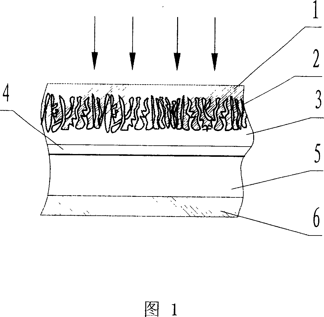
[0013] In order to illustrate the implementability of the present invention, in conjunction with accompanying drawing 1, enumerate an implementable scheme:

[0014] a. Using a P-type silicon substrate 5, according to the prior art, prepare a typical N silicon substrate by diffusing pentavalent elements on the side receiving light + P junction 4 (if an N-type silicon substrate is used, 3-valent elements must be diffused to prepare P + N junction. In addition to silicon wafers, N can be made on other suitable silicon substrate materials, such as silicon substrates obtained by epitaxy and silicon substrates obtained by chemical deposition. + P junction or P + N) to obtain an N-type silicon layer 3 .

[0015] b. On the non-light-receiving surface of the battery, prepare a thin layer with the same conductivity type as the semiconductor silicon on this surface with higher conductivity to form a back reflection field, and prepare the back electrode 6 on this basis.

[0016] c. Di...


PUM

PropertyMeasurementUnit
Scaleaaaaaaaaaa

Abstract

The invention relates to a solar cell, in order to solve the structural problem of the crystal silicon solar cell. The invention discloses a porous silicon layer structural crystal silicon solar cell, whose structure comprise in sequence: a N-type silicon layer, a P-type silicon layer, a back electrode, and a PN junction with photovoltaic effect formed on the boundary of the N-type silicon layer and the P-type silicon layer, which is charactered in that a nanometer porous silicon layer is provided on the silicon material surface at one side near to the light-receiving surface, and there are nesa structure on the surface of the nanometer porous silicon layer. The invention has made improvement in the existing structure, increasing a nanometer porous silicon layer, thus raising the photoelectric conversion efficiency of the solar cell. Because the dimension of quasi aperture and quasi hole wall of the nanometer porous silicon layer is between 2 nanometer to 300 nanometer, and the thickness of nanometer porous silicon layer is thinner, the thinner crystal silicon layer can be used to achieve the same light quantum turnout with a thicker crystal silicon layer. Therefore it saves the valuable semiconductor silicon material, and reduces the cost.

Description

technical field [0001] The invention relates to a solar cell, in particular to a crystalline silicon solar cell with a nano-crystal structure, and the nano-crystal is formed by a porous silicon structure. Background technique [0002] The structure of the existing crystalline silicon solar cell consists of light-receiving surface electrodes, anti-reflection film, N-type silicon and surface texture structure, P-type silicon, and a PN junction with photovoltaic effect formed at the junction of N-type silicon and P-type silicon. composed of electrodes. The structure of this crystalline silicon solar cell has the following problems: First, the surface texture structure of the cell is a periodic or non-periodic structure of protrusions or depressions, and the typical size of these microstructures is on the order of microns to reduce incident The reflection of light is for the purpose, and there is no quantum size effect; the second is that the P-type silicon material and the N-t...

Claims


Application Information

Patent Timeline
IPC IPC(8): H01L31/042H01L31/054
CPCY02E10/50Y02E10/52
Inventor 李涛勇刘琼张铃菊
Owner SHANGHAI SOLAR ENERGY S&T
Why Eureka
Try Eureka