
Eureka
For R&D, Eureka makes reading and utilizing patents & technical documents easy.
Eureka AIR
Designed for self-driven R&D workflows. Generate viable solutions, solve complex R&D challenges, empower your innovation with AI.

Eureka Materials
Designed for material experts only. Revolutionize your material R&D, from search, analyze, to developing new materials.

TechResearch
Generate reliable direction feasibility study reports for your R&D in just a few steps.

TechSeek
Discover and master advanced knowledge NOW. Basics, ideas, possibilities, all at once.

TechMind
As an expert in R&D Theories, TechMind can generates customized viable solutions instantly.

TechRisk
Analyze your overall solution with one click, know your potential R&D risks in advance.

TechMonitor
Get weekly tech updates, stay abreast of the latest tech innovations and key insights.
A method for manufacturing of enhancement type ZnO channel layer thin film transistor with ammonia doping
A thin-film transistor and channel layer technology, applied in electrical components, semiconductor/solid-state device manufacturing, circuits, etc., can solve problems such as poor doping uniformity, reduce carrier concentration, limit application and promotion, and achieve controllability Good, simple preparation process, good process compatibility
- Summary
- Abstract
- Description
- Claims
- Application Information
AI Technical Summary
Problems solved by technology
Method used
Image

Examples
Embodiment 1
[0024] This embodiment is to prepare a ZnO channel layer thin film transistor.
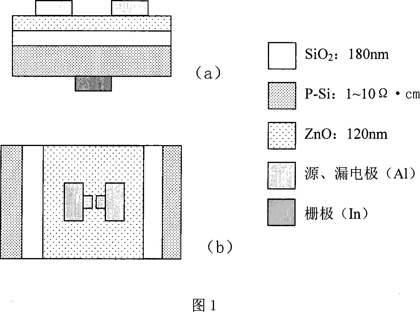
[0025] First, select a P-type Si sheet (p-Si) with a resistivity of 1-10Ω·cm as the substrate, and use it as the gate of the thin film transistor, and grow 180nm on the substrate by using a conventional dry oxygen oxidation process on the p-Si surface. Thick silicon dioxide acts as an insulating layer for thin-film transistors (Figure 1). Or directly use ITO glass as the substrate, the ITO film on the glass as the gate, and re-grow HfO on the ITO film 2 、Al 2 o 3 or Y 2 o 3 The insulating layer of a dielectric film.
[0026] Put the above-mentioned substrate grown with an insulating layer into the vacuum chamber of the vacuum system, and pre-evacuate the vacuum system to 10 -6 Pa, and then slowly heat the substrate to make the substrate temperature reach 400°C, oxygen (O 2 ) and ammonia (NH 3 ) under the condition of adjusting the ratio of 1:1, deposit high-quality nitrogen-doped ZnO chann...
Embodiment 2
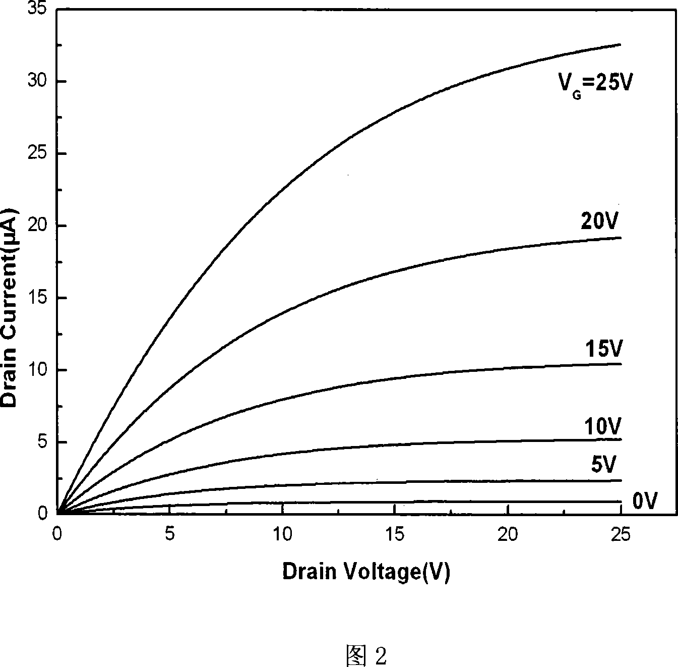
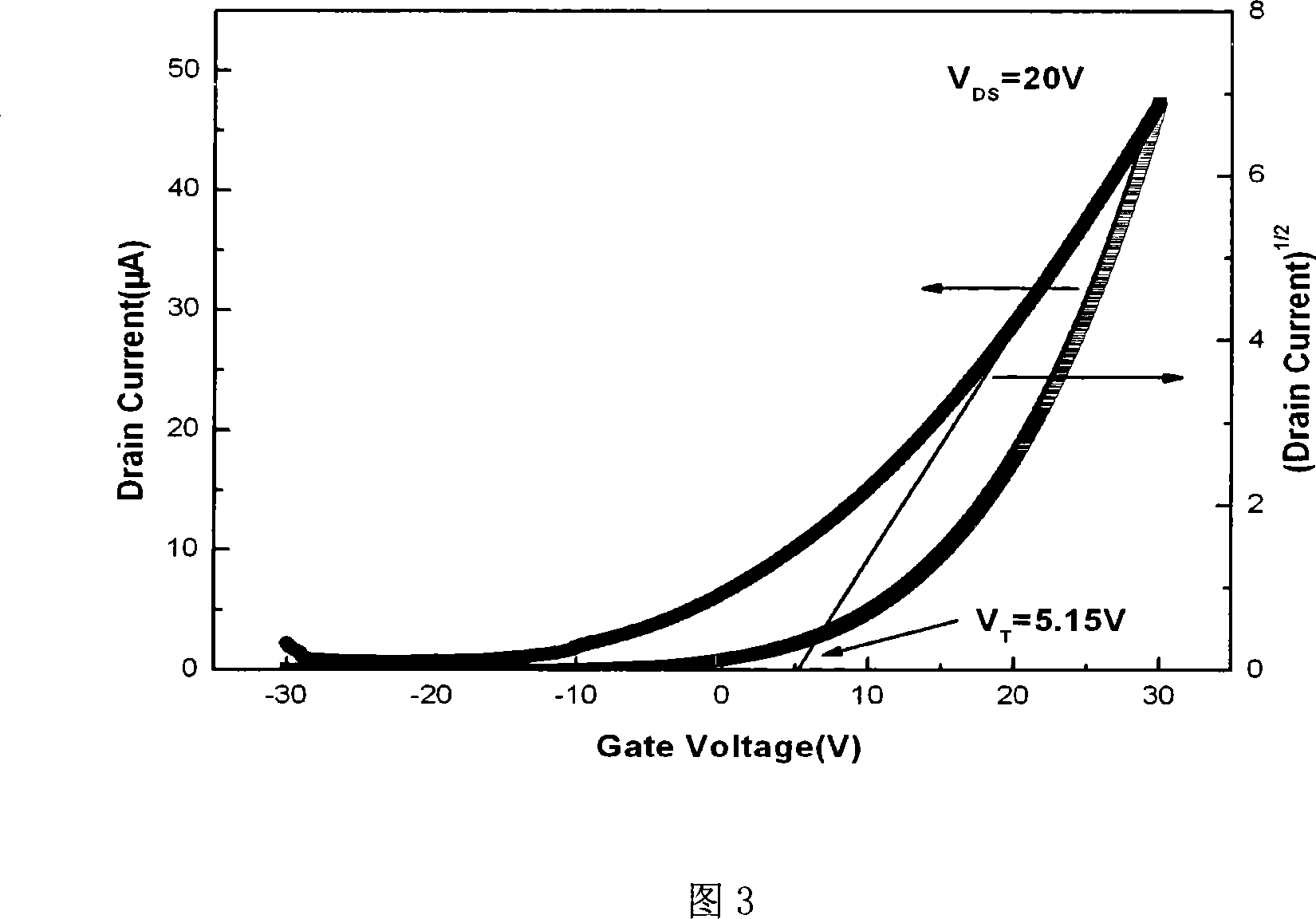
[0038] The difference between this embodiment and embodiment 1 is that the ZnO target in step 3 is replaced with a Zn-Mg-O, Zn-Sn-O or Zn-In-O target, and the others are the same as in embodiment 1, namely Nitrogen-doped Zn-Mg-O, Zn-Sn-O, and Zn-In-O thin films are grown under a mixed atmosphere of ammonia and oxygen as the channel layer of ZnO thin film transistors, which can also obtain excellent electrical properties at low temperatures. Enhanced device. The electrical test results still have electrical properties similar to those in Figure 2, Figure 3, and Figure 4.
Embodiment 3
[0040] The difference between this embodiment and embodiment 1 is that the Si-based substrate in step 1 is changed to ITO glass, and the ITO film is used as the grid. Others are the same as in embodiment 1, and a layer of high dielectric constant insulating Thin films such as HfO 2 、Al 2 o 3 or Y 2 o 3 etc., and then grow a nitrogen-doped ZnO film on the insulating layer and prepare source and drain electrodes. The electrical test results still have electrical properties similar to those in Figure 2, Figure 3, and Figure 4.
PUM
 Abstract
Description
Claims
Application Information
 - R&D Engineer
- R&D Manager
- IP Professional
- Industry Leading Data Capabilities
- Powerful AI technology
- Patent DNA Extraction
Browse by: Latest US Patents, China's latest patents, Technical Efficacy Thesaurus, Application Domain, Technology Topic, Popular Technical Reports.
© 2024 PatSnap. All rights reserved.Legal|Privacy policy|Modern Slavery Act Transparency Statement|Sitemap|About US| Contact US: help@patsnap.com