Production of coarsening electrode for high-brightness packed LED chip and vertical LED chip

A high-brightness, metal electrode technology, applied in circuits, electrical components, semiconductor devices, etc., can solve problems such as reducing the external quantum efficiency of LED devices

Inactive Publication Date: 2007-11-21
AQUALITE CO LTD
View PDF0 Cites 65 Cited by
  • Summary
  • Abstract
  • Description
  • Claims
  • Application Information

AI Technical Summary

Problems solved by technology

Only about less than 20% of the light energy enters the air from the ITO medium, which greatly reduces the external quantum efficiency of the LED device

Method used


Image

  • Production of coarsening electrode for high-brightness packed LED chip and vertical LED chip
  • Production of coarsening electrode for high-brightness packed LED chip and vertical LED chip
  • Production of coarsening electrode for high-brightness packed LED chip and vertical LED chip

Examples


Embodiment Construction

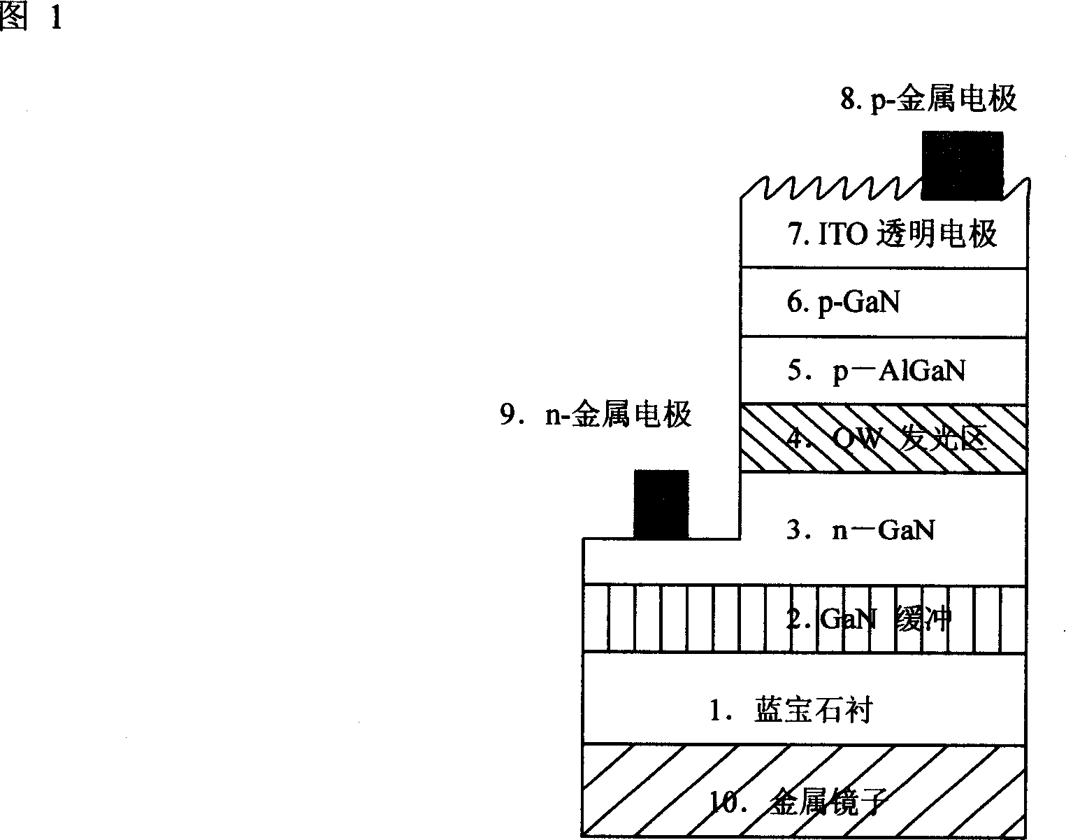
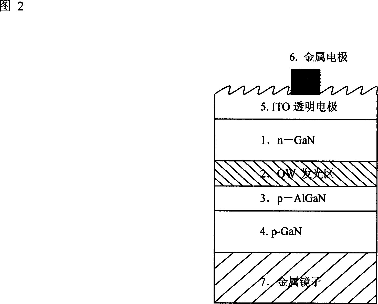
[0012] One of the novel light-emitting diodes of the present invention, comprising a sapphire substrate 1, a GaN buffer layer 2, an n-type GaN layer 3, an InGaN / GaN multiple quantum well (MQWs) active layer (light-emitting layer) 4, and a p-AlGaN waveguide layer 5 , p-type GaN layer 6, p-type ohmic-contact transparent electrode 7, p-type ohmic-contact transparent electrode 8, n-type ohmic-contact electrode 9 and metal layer mirror 10. ITO is used as the material, and the surface of the ITO film is roughened by natural lithography and dry etching.

[0013] In order to realize the above-mentioned light-emitting diodes, a method for preparing a high-brightness light-emitting diode of the present invention comprises the following steps:

[0014] (1) Using MOCVD epitaxy to grow GaN-based LED structure epitaxial wafers, the lower lining is blue sapphire (Al 3 o 2 );

[0015] (2) Deposit ITO film on the epitaxial wafer by electron beam evaporation;

[0016] (3) Apply natural lith...


PUM


Abstract

This is a process method for a high brightness LED chip applying nature light etching and ICP dry etching technology to the transparent conducting film on traditional and vertical LED on GaN base to increase illumination efficiency.

Description

technical field [0001] The invention relates to a process method for manufacturing a high-brightness LED chip by a gallium nitride (GaN) semiconductor, in particular to roughening the surface of a transparent conductive film ITO to improve the light extraction efficiency of the LED chip, and belongs to the technical field of nano-processing and semiconductor lighting. Background technique [0002] External quantum efficiency is the main technical bottleneck of high-brightness LED chips, and its size is equal to the product of internal quantum efficiency and light escape rate. Currently, the internal quantum efficiency of commercial LEDs is close to 100%, but the external quantum efficiency is only 3-30%. This is mainly due to the low escape rate of light. The factors that cause the low escape rate of light include: the absorption of light by lattice defects; the absorption of light by the substrate; the loss of light at each interface due to total reflection during the exit...

Claims


Application Information

Patent Timeline
Patent Type & Authority Applications(China)
IPC IPC(8): H01L33/00
Inventor 靳彩霞姚雨董志江黄素梅
Owner AQUALITE CO LTD
Why Eureka
Try Eureka