

Blanking device for optical film and blanking method for optical film
An optical film and blanking technology, applied in metal processing and other directions, can solve the problems of not being able to effectively prevent dust adhesion and easy generation of dust, and achieve the effect of preventing electrification of the optical film and being easy to manufacture
- Summary
- Abstract
- Description
- Claims
- Application Information
AI Technical Summary
Problems solved by technology
Method used
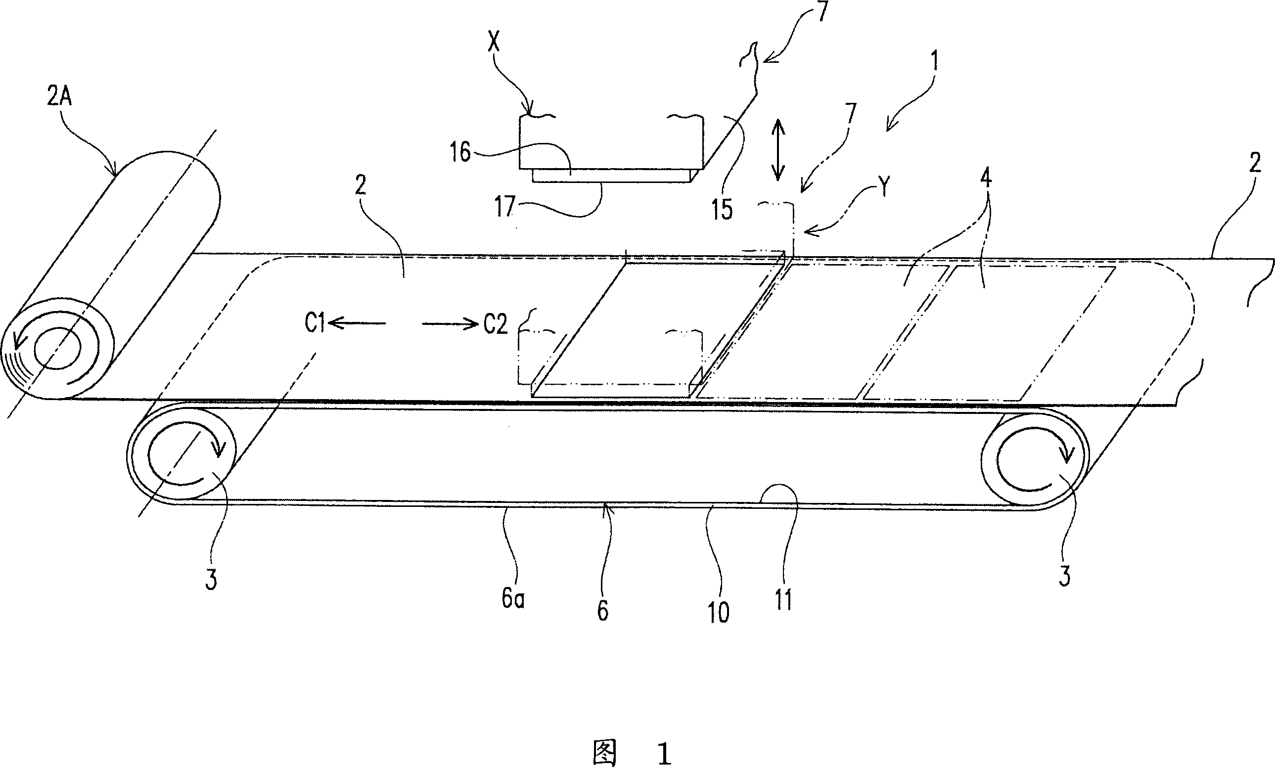
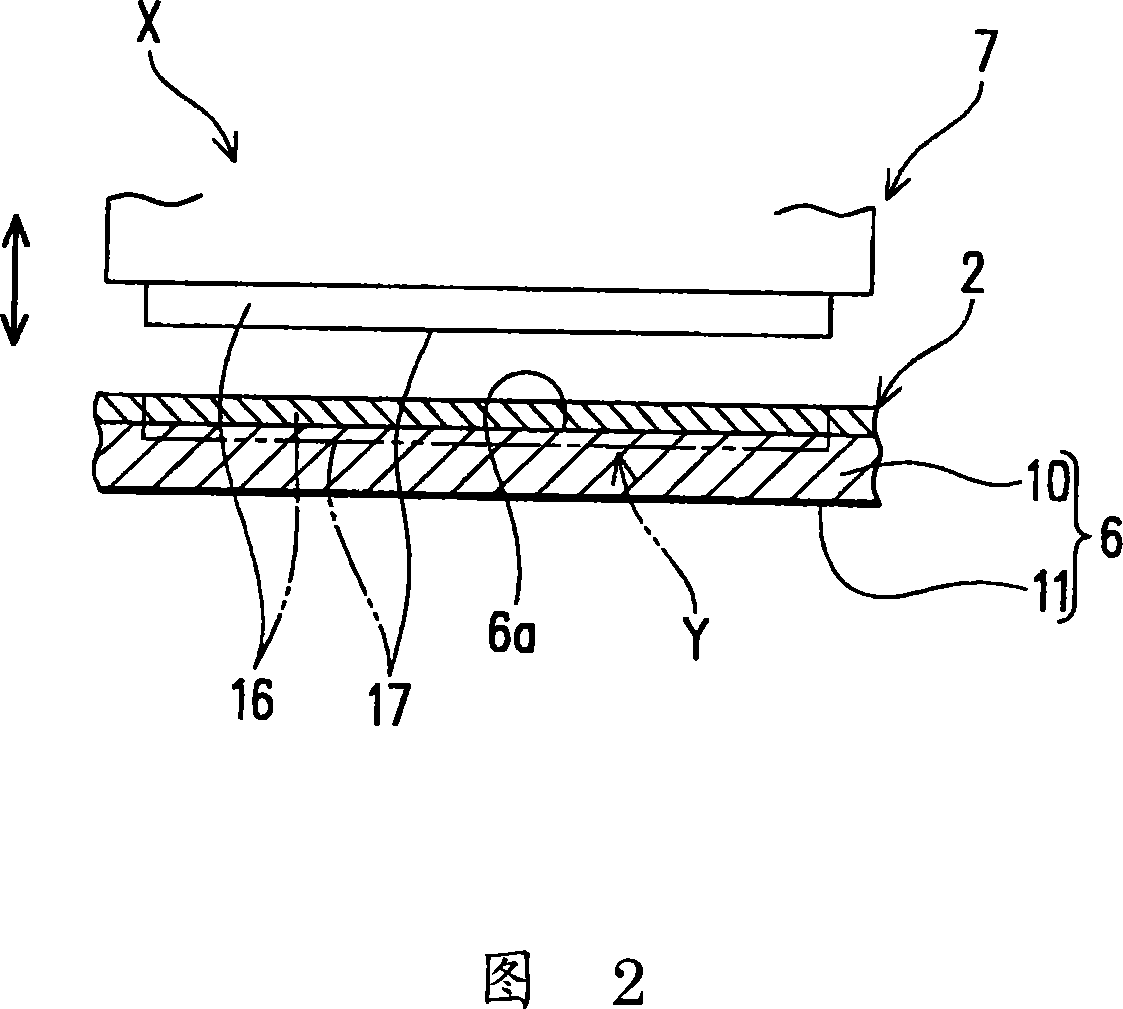
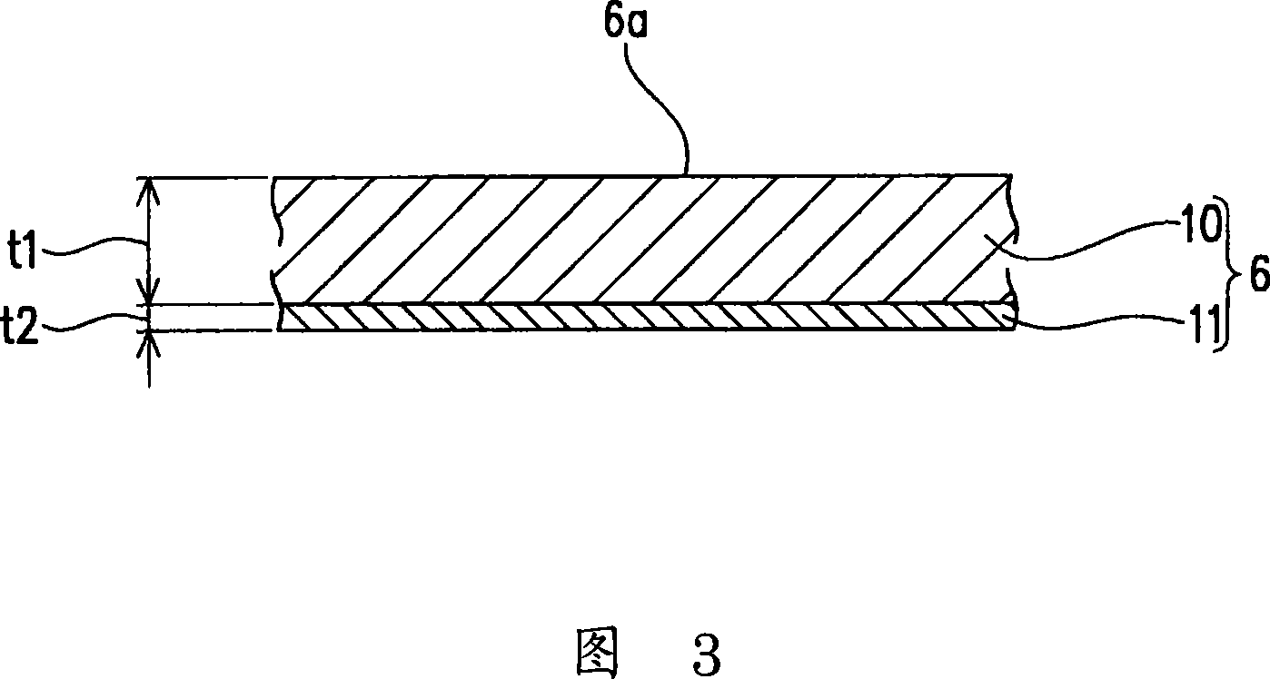
Image

Examples
Embodiment 1
[0056] (When organic solvent-soluble polyaniline is used for the polypropylene film of the conductive treatment layer 11)
[0057] 6000 g of distilled water, 360 ml of 36% hydrochloric acid, and 400 g (4.295 moles) of aniline were sequentially added to a 101 (10 liter) separable flask equipped with a stirring device, a thermometer, and a straight pipe joint to dissolve the aniline. Separately, while cooling with ice water, 434 g (4.295 mol) of 97% concentrated sulfuric acid was added and mixed to 1493 g of distilled water in a beaker to prepare a sulfuric acid aqueous solution. This sulfuric acid aqueous solution was put into the said separable flask, and the whole flask was cooled to -4 degreeC with the cryostat.
[0058] Then, 980 g (4.295 mol) of ammonium peroxodisulfate was added and dissolved in 2293 g of distilled water in a beaker to prepare an aqueous oxidizing agent solution. Cool the flask as a whole in a low-temperature constant temperature tank, and keep the tempe...
Embodiment 2
[0066] (When a mixture of organic solvent-soluble polyaniline and binder polymer is used for the polyethylene terephthalate film of the conductive treatment layer 11)
[0067] Prepare 100 parts by weight of polyaniline obtained in Example 1, 200 parts of malonic acid, 100 parts of linear saturated polyester resin "Byron RV-290" manufactured by Toyobo Co., Ltd., and 1.0% by weight of N-methyl- 2-pyrrole solution to make a coating solution.
[0068] This coating solution was applied to one side of a polyethylene terephthalate film with a thickness of 480 μm, and dried in a hot air dryer at 80° C. for 2 minutes to form a conductive treatment layer 11 with a thickness of 0.1 μm.
[0069] The obtained film had a surface resistance of 9 × 10 7 Ω / □. The surface roughness Ra of the surface of the polyethylene terephthalate film on the side opposite to the conductive treatment layer 11 was 0.067 μm, and Rz was 0.351 μm.
Embodiment 3
[0071] (When poly 3,4-dioxythiophene is used for the polypropylene film of the conductive treatment layer 11)
[0072] A 5% by weight isopropanol solution of 100 parts of 3,4-dioxythiophene and 500 parts of iron p-toluenesulfonate was applied to one side of a polypropylene film having a thickness of 500 μm, and left to stand at room temperature. Polymerization proceeds to form a thin film on the substrate. This was washed with running water and dried to form a conductive treatment layer 11 with a thickness of 0.05 μm.
[0073] The obtained film had a surface resistance of 3 × 10 8 Ω / □. The surface roughness of the surface of the polypropylene film on the opposite side to the conductive treatment layer 11 was the surface roughness of the non-conductive treatment surface as in Example 1 and Example 2.
PUM
| Property | Measurement | Unit |
|---|---|---|
| Surface resistance | aaaaa | aaaaa |
| Surface roughness | aaaaa | aaaaa |
| Surface resistance | aaaaa | aaaaa |
Abstract
Description
Claims
Application Information