
Thin film structure for reducing laser direct writing photo-etching point or line width and its preparation method
A thin-film structure and laser direct writing technology, which is applied in laser welding equipment, microlithography exposure equipment, optomechanical equipment, etc., can solve problems such as complex process, high cost, and difficult industrialization direction
- Summary
- Abstract
- Description
- Claims
- Application Information
AI Technical Summary
Problems solved by technology
Method used
Image

Examples
preparation example Construction
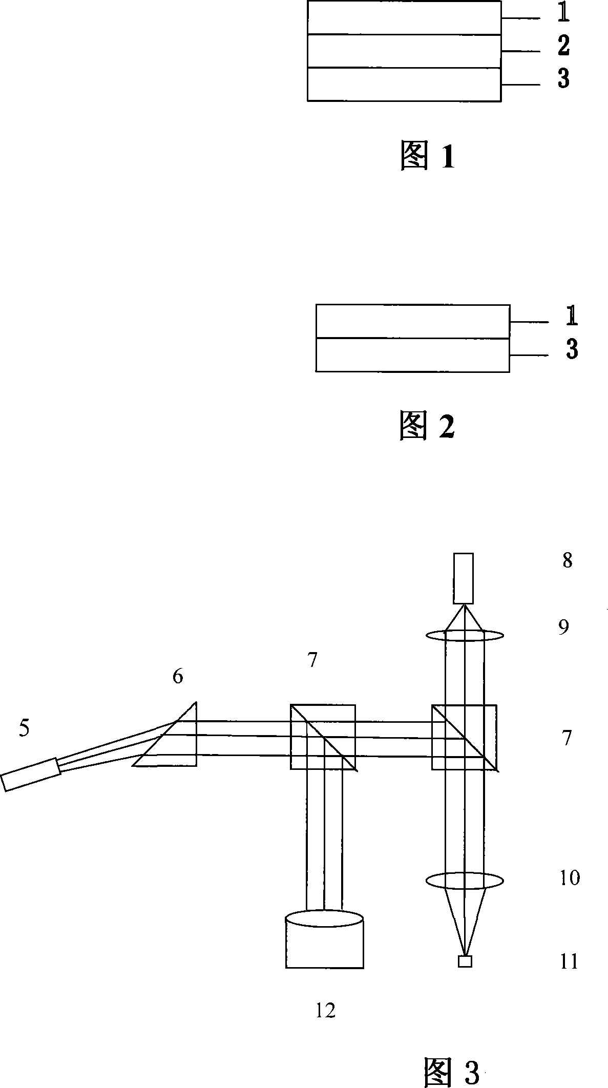
[0019] The preparation method of the thin film structure reducing laser direct writing lithography point or line width is characterized in that it comprises the following steps:
[0020] ①Put the glass substrate 3 into absolute alcohol, and clean it two to three times with an ultrasonic generator, 10 minutes each time;
[0021] ②Put the cleaned glass substrate into the sputtering chamber of the high-vacuum magnetron sputtering equipment after drying, and vacuumize. When the background vacuum in the sputtering chamber drops to 6.0*10 -4 At Pa, argon is passed through, and the argon pressure is maintained at 0.6-1.0Pa;
[0022] ③ preparing the buffer layer 2 on the glass substrate 3 by DC magnetron sputtering;
[0023] ④ Prepare the inorganic phase change thin film layer 1 on the buffer layer 2 by DC magnetron sputtering method.
PUM
| Property | Measurement | Unit |
|---|---|---|
| Thickness | aaaaa | aaaaa |
Abstract
Description
Claims
Application Information