Method for fabricating pixel structure

A technology of a pixel structure and a manufacturing method, which is applied in the fields of semiconductor/solid-state device manufacturing, optics, instruments, etc., can solve the problems of high cost of large-size photomasks, the manufacturing cost of pixel structure 90 cannot be reduced, and the cost of photomasks is expensive. low cost effect

Inactive Publication Date: 2008-02-06
AU OPTRONICS CORP
View PDF0 Cites 10 Cited by
  • Summary
  • Abstract
  • Description
  • Claims
  • Application Information

AI Technical Summary

Problems solved by technology

Since the cost of the photomask is very expensive, and each photomask manufacturing process must use a photomask with different patterns, if the number of photomask manufacturing processes cannot be reduced, the manufacturing cost of the pixel structure 90 will not be reduced.
[0005] In addition, as the size of TFT liquid crystal display panels increases, the size of the photomask used to manufacture the TFT array substrate will also increase accordingly, and the large-sized photomask will be more expensive in terms of manufacturing cost, making the pixel structure 90 Manufacturing costs cannot be effectively reduced

Method used


Image

  • Method for fabricating pixel structure
  • Method for fabricating pixel structure
  • Method for fabricating pixel structure

Examples


no. 1 example

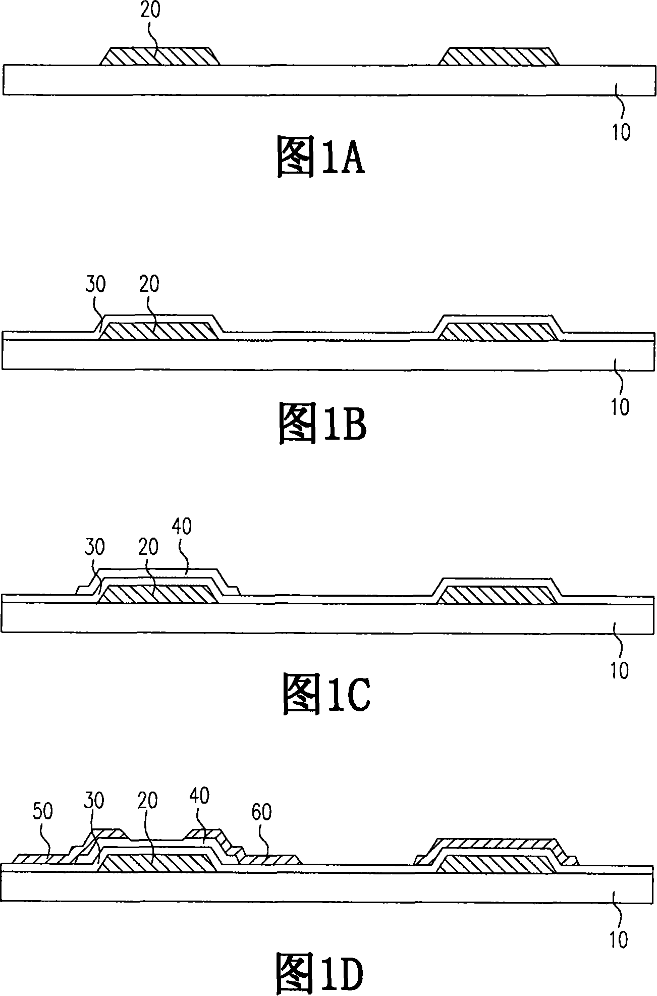
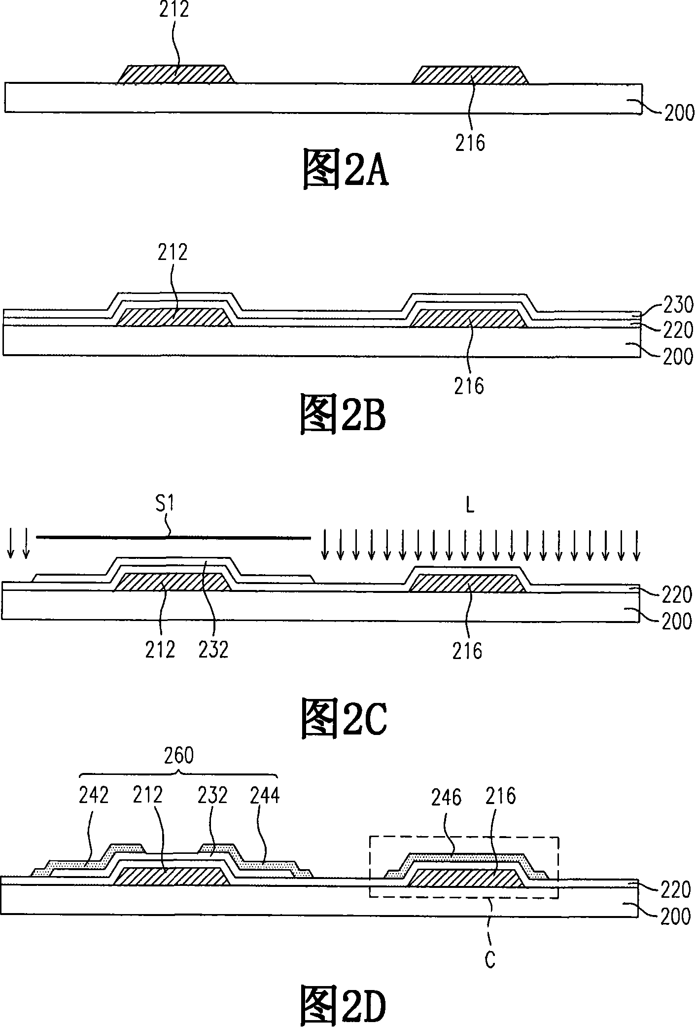
[0056] 2A to 2G are schematic diagrams of a manufacturing method of a pixel structure of the present invention. Referring to FIG. 2A , firstly, a substrate 200 is provided, and the material of the substrate 200 is hard or soft materials such as glass and plastic. Next, a gate 212 is formed on the substrate 200 . In this embodiment, it also includes forming the lower capacitor electrode 216 while forming the gate 212 .

[0057] Next, referring to FIG. 2B , a gate dielectric layer 220 is formed on the substrate 200 to cover the gate electrode 212 and the lower capacitor electrode 216, wherein the gate dielectric layer 220 is, for example, formed by chemical vapor deposition (CVD) or other suitable film deposition techniques, and the material of the gate dielectric layer 220 is, for example, a dielectric material such as silicon oxide, silicon nitride, or silicon oxynitride. Next, a semiconductor layer 230 is formed on the gate dielectric layer 220 . In this embodiment, the ma...

no. 2 example

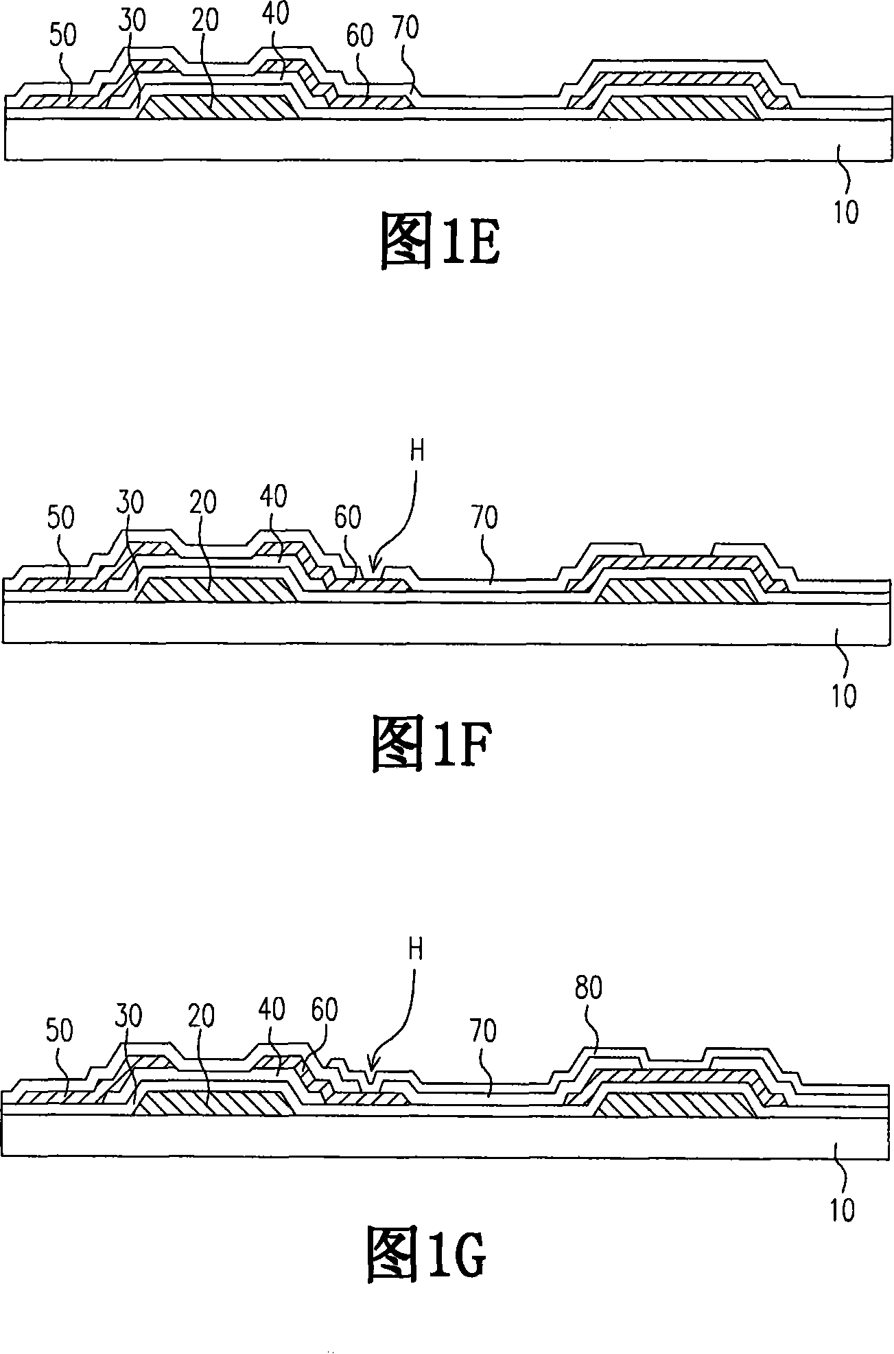
[0067] 6A to 6H are schematic diagrams of a manufacturing method of the pixel structure in the second embodiment of the present invention. Since the steps in FIG. 6A-FIG. 6E are similar to those in FIG. 2A-FIG. 2E of the first embodiment, their descriptions are omitted here.

[0068] Referring to FIG. 6F , after the patterned protection layer 272 is formed, the patterned protection layer 272 is baked so that the patterned protection layer 272 has a mushroom-shaped top surface M. Referring to FIG. The patterned passivation layer 272 after baking exhibits a pattern in which the top surface of the patterned passivation layer 272 is slightly larger than the bottom surface thereof, so that the top surface of the patterned passivation layer 272 substantially presents the above-mentioned mushroom-shaped top surface M. It is worth mentioning that in practice, manufacturing process errors such as temperature, heating speed, and heating time of the baking process must be considered. The...


PUM

PropertyMeasurementUnit
wavelengthaaaaaaaaaa

Abstract

The present invention relates to a manufacturing method for the image element structure, which comprises the steps below. Firstly, the present invention provides a basal plate and form a grid on the basal plate, and then the a door dielectric layer is formed on the basal plate to cover the grid, and then a semiconductor layer is formed on the door dielectric layer, and the present invention provides a first shield cover extending partial semiconductor layer above the semiconductor layer, and the present invention uses the laser irradiation to remove partial semiconductor layer to form a channel layer, and then the present invention form a source electrode and a drain electrode on the channel layer on two sides of the grid, then the present invention form a design protecting layer to cover the channel and is uncovered from the drain electrode. Finally the present invention form a conductive layer to cover the design protecting layer and the uncovered drain electrode, and the present invention makes the conductive layer designed through the design protecting layer to form the image element electrode.

Description

technical field [0001] The present invention relates to a method for manufacturing a pixel structure, and in particular to a method for manufacturing a pixel structure using a laser ablation process to manufacture a semiconductor layer. Background technique [0002] A display is a communication interface between people and information, and flat-panel displays are currently the main development trend. There are mainly the following types of flat panel displays: organic electroluminescence display, plasma display panel, and thin film transistor liquid crystal display. Among them, thin film transistor liquid crystal display is the most widely used. Generally speaking, a thin film transistor liquid crystal display is mainly composed of a thin film transistor array substrate, a color filter substrate and a liquid crystal layer. Wherein, the thin film transistor array substrate includes a plurality of scan lines (scan lines), a plurality of data lines (data lines) and a pluralit...

Claims


Application Information

Patent Timeline
Patent Type & Authority Applications(China)
IPC IPC(8): H01L21/84H01L21/3213G02F1/1362
Inventor 廖金阅杨智钧黄明远林汉涂石志鸿廖达文蔡佳琪
Owner AU OPTRONICS CORP
Why Eureka
Try Eureka