Method for making lead and tin alloy protruding point

A production method and lead-tin technology, which are applied in semiconductor/solid-state device manufacturing, electrical components, and electrical solid-state devices, etc., can solve the problems of slow plating rate, long production cycle, and increased labor cost, avoiding bubbles, The effect of improving welding performance and saving costs

Inactive Publication Date: 2008-02-13
SEMICON MFG INT (SHANGHAI) CORP +1
View PDF1 Cites 7 Cited by
  • Summary
  • Abstract
  • Description
  • Claims
  • Application Information

AI Technical Summary

Problems solved by technology

However, the above method can only eliminate relatively large air bubbles, and after two printings and two reflows, the process is more complicated
[0008] 0.5 to 1A / dm have also been tried in prior art 2 The method of electroplating lead-tin alloy solder with a higher current density can eliminate the air bubbles in the lead-tin alloy bumps, but the current is too low, the plating rate will slow down, the production cycle will be longer, the output rate will be lower, and the labor cost will increase; if the electroplating rate is increased current density without avoiding the formation of air bubbles in the solder bump

Method used


Image

  • Method for making lead and tin alloy protruding point
  • Method for making lead and tin alloy protruding point
  • Method for making lead and tin alloy protruding point

Examples


Embodiment Construction

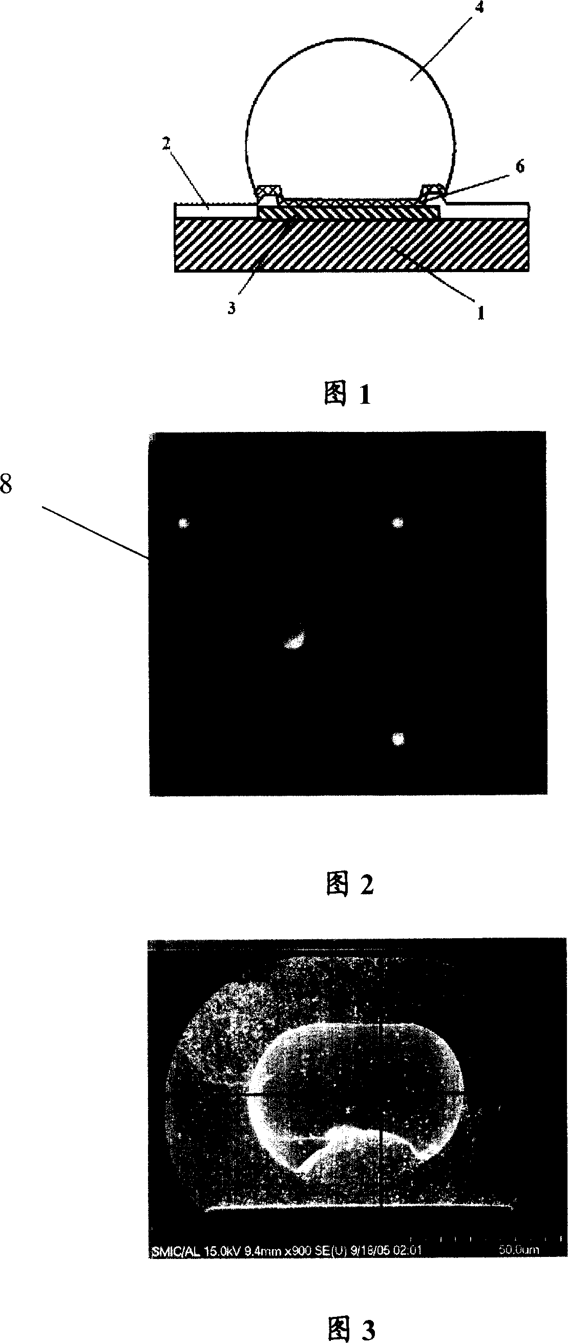
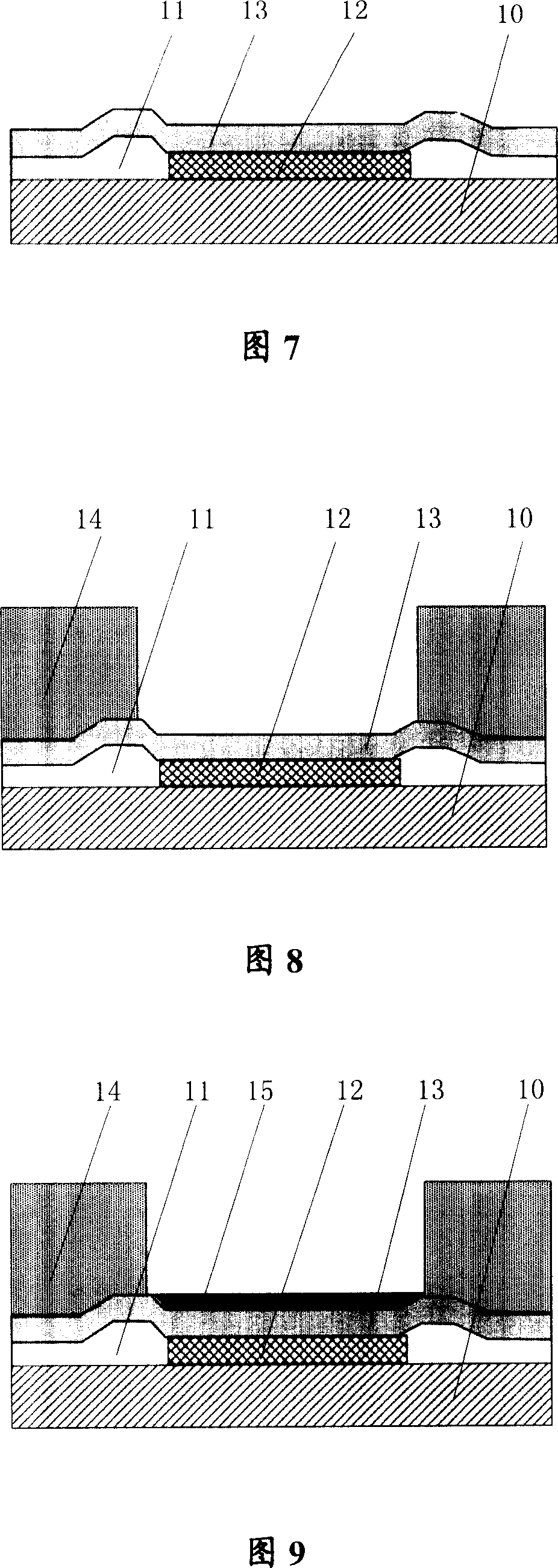
[0043] Aiming at the manufacturing method of the lead-tin alloy bump adopted in the present invention, a detailed description will be given below in conjunction with the accompanying drawings and embodiments.

[0044]In the prior art, materials such as titanium, titanium-tungsten alloy, copper, and nickel are usually selected as the under-bump metal material in the solder bump process, and metal nickel is more commonly used when depositing lead-tin alloy bumps by electroplating.

[0045] When adopting lead-tin alloy as bump solder, and adopting the method for electroplating to deposit lead-tin alloy bump, usually adopt the electroplating solution of methanesulfonic acid system, lead ion concentration (Pb 2+ ) is 40 to 60g / L, tin ions (Sn 2+ ) concentration is 5 to 10g / L, methanesulfonic acid is used as the complexing agent in the solution, and the concentration is 200 to 300g / L. When electroplating lead-tin alloy solder, the current density is 3A / dm 2 up to 10A / dm 2 , the r...


PUM

PropertyMeasurementUnit
current densityaaaaaaaaaa

Abstract

The present invention provides a pewter bump manufacturing method comprising the following steps: to deposit an under bump metal layer on wafer; to form a photoresist layer on the under bump metal layer, and to form a photoresist opening by exposure and develop; to form a transitional pewter layer on the under bump metal layer located at the photoresist opening; to electroplate a wiping solder on the transitional pewter layer; to remove the photoresist and the under bump metal layer; to backflow the wiping solder to form pewter bump. The process of forming the transitional pewter layer is of an electroplating process, the electric current density is 0.1A/dm2 to 1A/dm2, and the time is 1-5 minutes. The density of the formed transitional pewter layer is 0.2um to 4um. The method of the present invention avoids bubble formation in pewter bump solder in electroplating process.

Description

technical field [0001] The invention relates to a method for manufacturing bumps in semiconductor manufacturing processes, and more specifically, relates to a method for manufacturing bumps of lead-tin alloys, which avoids bubbles in the solder during the process of electroplating bump solder. Background technique [0002] With the continuous development of integrated circuit technology, electronic products are increasingly developing in the direction of miniaturization, intelligence, high performance and high reliability. The integrated circuit packaging not only directly affects the performance of integrated circuits, electronic modules and even the whole machine, but also restricts the miniaturization, low cost and reliability of the entire electronic system. With the gradual reduction of the size of the integrated circuit chip and the continuous improvement of the integration level, the electronic industry has put forward higher and higher requirements for the packaging ...

Claims


Application Information

Patent Timeline
Patent Type & Authority Applications(China)
IPC IPC(8): H01L21/60H01L21/28
CPCH01L24/11H01L2224/05022H01L2224/05572H01L2224/11H01L2224/1147H01L2224/13H01L2224/13139H01L2924/01322H01L2924/14H01L2924/00H01L2924/00012
Inventor 丁万春
Owner SEMICON MFG INT (SHANGHAI) CORP
Why Eureka
Try Eureka