LED encapsulation structure and method

A technology of light-emitting diodes and packaging structures, which is applied in the direction of electrical components, electrical solid devices, circuits, etc., can solve problems such as low production efficiency, unfavorable large-scale production, and adverse effects of phosphor powder, so as to improve reliability and improve light and color quality and luminous uniformity, the effect of avoiding adverse effects

Inactive Publication Date: 2008-02-13
GUANGDONG REAL FAITH OPTO
View PDF0 Cites 19 Cited by
  • Summary
  • Abstract
  • Description
  • Claims
  • Application Information

AI Technical Summary

Problems solved by technology

Because each light-emitting chip has to be pasted with cured film, the production efficiency is very low, which is not conducive to large-scale production; and

Method used


Image

  • LED encapsulation structure and method

Examples


Embodiment 1

[0010] Embodiments of the present invention are further described below in conjunction with the accompanying drawings:

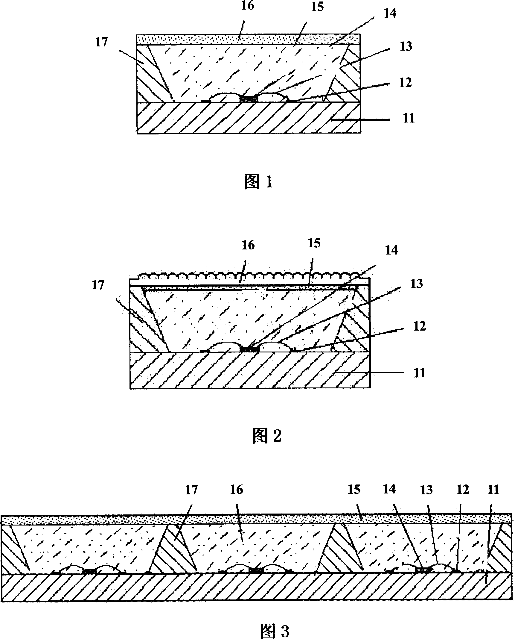
[0011] See Figure 1, the specific packaging process is as follows:

[0012] A. The GaN blue LED chip 14 is welded to the chip area of ​​the copper-clad ceramic heat dissipation substrate 11 by low-temperature solder, and connected to the pad 12 by the metal lead 13;

[0013] B. Making a transparent body 15 on the Blu-ray chip 14 through a molding process of silica gel;

[0014] C. bonding the aluminum reflective cup 17 around the blue chip 14;

[0015] D. Add aluminum yttrium garnet (YAG) yellow fluorescent powder 18 into the glass-ceramic raw material, mix it evenly, sinter and form it, and then cut, grind and polish it to prepare the fluorescent powder-containing substrate 16;

[0016] E. Fix the phosphor-containing substrate 16 to the top of the reflective cup 17 by glue.

Embodiment 2

[0018] Embodiment 2 is the same as Embodiment 1, except that a microlens array is formed on the surface of the glass substrate 16 through a micromachining process, and the phosphor 18 is deposited on the substrate 16 by evaporation deposition or glue. Adhesive surface, finally the substrate 16 is fixed to the top of the reflective cup 17 by glue, see FIG. 2 .

Embodiment 3

[0020] Embodiment 3 is the same as Embodiment 1, except that the single-color light-emitting chips 14 are in an array structure. The chip 14 is welded to the chip area of ​​the heat dissipation substrate 11 to form a chip array, and is connected to the pad 12 through the metal lead 13, and the transparent body 15 is formed on the chip array 14 through a glue injection molding process, and then the reflective cup array 17 is fixed on the on the heat dissipation substrate 11 , corresponding to the chip 14 and the transparent body 15 , and finally the phosphor-containing substrate 16 is fixed on the top of the reflective cup array 17 . See Figure 3.

[0021] In each of the above embodiments, the surface of the substrate can also be a regular rough surface, and the light-emitting chip can also be a purple light chip or an ultraviolet light chip, and the corresponding fluorescent powder is RGB (red, green, blue) three-color fluorescent Powder; welding and anodic bonding can also b...


PUM


Abstract

A packaging structure and method of light-emitting diode mainly comprises a monochromatic LED chip, a lead wire, a substrate, a condensing lens, a phosphor, a reflecting bowl and a radiating substrate. The invention is characterized in that the chip is formed by the sintering process after adding the phosphor into the raw material and uniform mixing them, the substrate containing the phosphor is fixed at the top surface of the reflecting bowl around the chip, and the LED chip is fixed in the chip area of the radiating substrate by metal welding, anodic bonding or resin bonding. The invention has the advantages that the invention can accurately control the dose of phosphor, promote the light quality and luminescence uniformity of white LED after packaging, meanwhile avoid the adverse effect on the phosphor from high temperature during use, and promote the reliability of LED after packaging.

Description

technical field [0001] The invention relates to a manufacturing method of a semiconductor device, a light emitting diode packaging structure and method, in particular to a white light LED packaging structure and method. technical background [0002] The existing high-brightness white light-emitting diode LED is formed by mixing various colors of light. For example, red, green and blue chips are combined to form white light through optical lens, or purple or ultraviolet light is used to excite RGB (red, green and blue) phosphors to obtain white light, or blue light is used to excite yellow phosphors to obtain white light. Among them, the use of blue LED chips to excite YAG yellow phosphors to produce white light is the most widely used. YAG yellow phosphors are mixed into epoxy resin or silica gel, mixed evenly, and then coated on blue chips by coating or dispensing. The disadvantage of this method is that if the coating dose of the yellow phosphor is not accurately controll...

Claims


Application Information

Patent Timeline
IPC IPC(8): H01L33/00H01L25/00H01L21/50H01L33/48H01L33/50
CPCH01L2224/48091H01L2224/48227
Inventor 刘胜陈明祥罗小兵甘志银
Owner GUANGDONG REAL FAITH OPTO
Why Eureka
Try Eureka