Wafer packaging construction with array connecting pad and method of manufacturing the same

A chip packaging and array technology, applied in semiconductor/solid-state device manufacturing, electrical components, electric solid-state devices, etc., can solve the problems of forming antenna effect, affecting product reliability, general products and methods without suitable structures and methods, etc. Achieve the effect of avoiding scratches or wear, improving anti-rust effect, and avoiding antenna effect

Inactive Publication Date: 2008-02-27
CHIPMOS TECH INC
View PDF0 Cites 30 Cited by
  • Summary
  • Abstract
  • Description
  • Claims
  • Application Information

AI Technical Summary

Problems solved by technology

These exposed surfaces 116 cannot be covered and protected by the electroplating layer 115 according to the existing manufacturing process, so it is easy to start rusting from these exposed surfaces 116, which affects the reliability of the product
In addition, the exposed surface 116 of these pins 111 will also cause interference to high-frequency signals, forming an antenna effect
Furthermore, as shown in FIG. 2, since each outer end of these pins 111 must extend to the side of the sealing body 140, the arrangement of these pins can only be single row or multi-row staggered. arrangement, and cannot further achieve high-density chip packaging
[0005] It can be seen that the above-mentioned existing chip packaging structure and its manufacturing method obviously still have inconvenience and defects in product structure, manufacturing method and use, and need to be further improved urgently.
In order to solve the above-mentioned problems, the relevant manufacturers have tried their best to find a solution, but no suitable design has been developed for a long time, and there is no suitable structure and method for general products and methods to solve the above-mentioned problems. This is obviously a problem that relevant industry players are eager to solve

Method used


Image

  • Wafer packaging construction with array connecting pad and method of manufacturing the same
  • Wafer packaging construction with array connecting pad and method of manufacturing the same
  • Wafer packaging construction with array connecting pad and method of manufacturing the same

Examples


no. 1 Embodiment

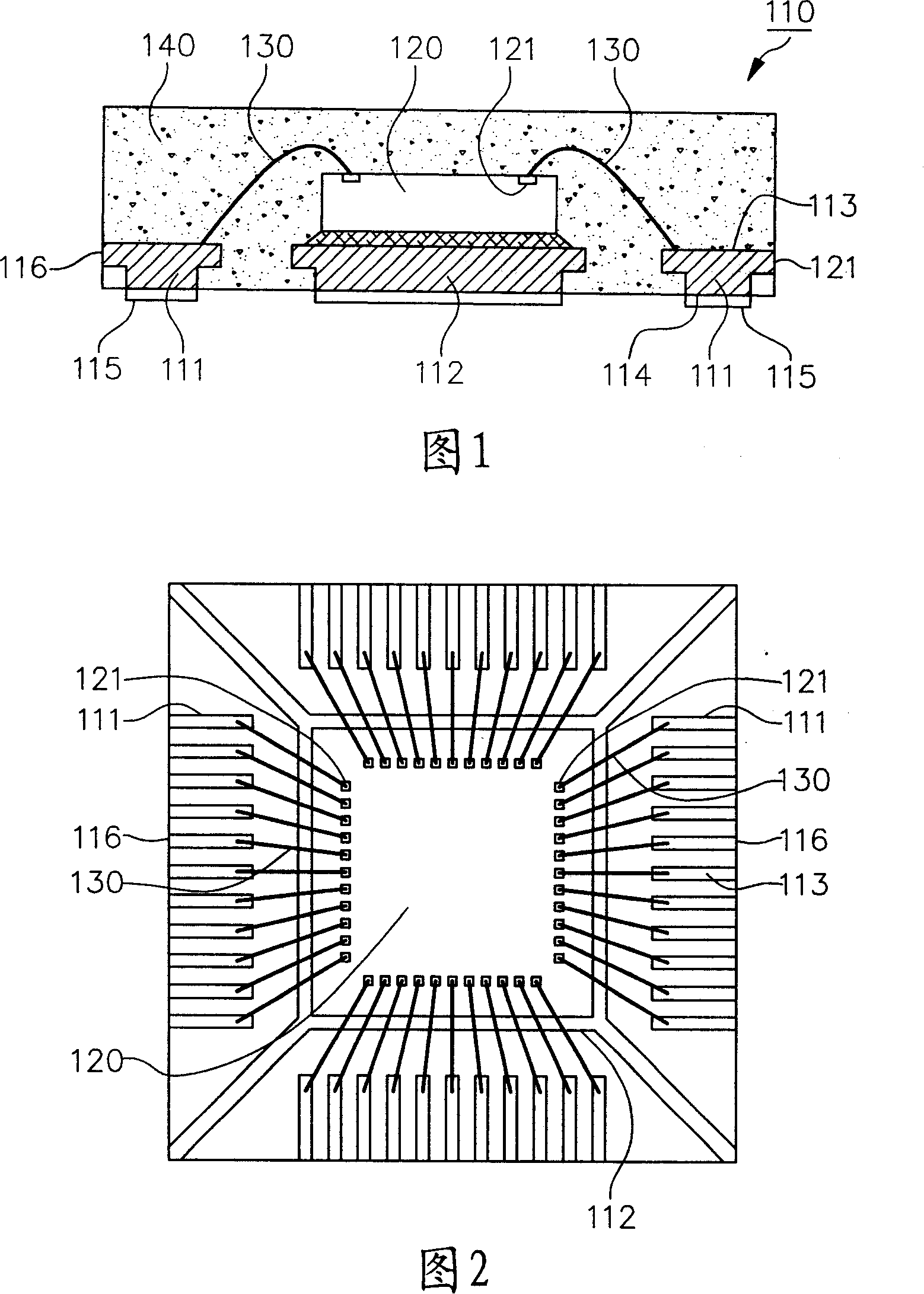
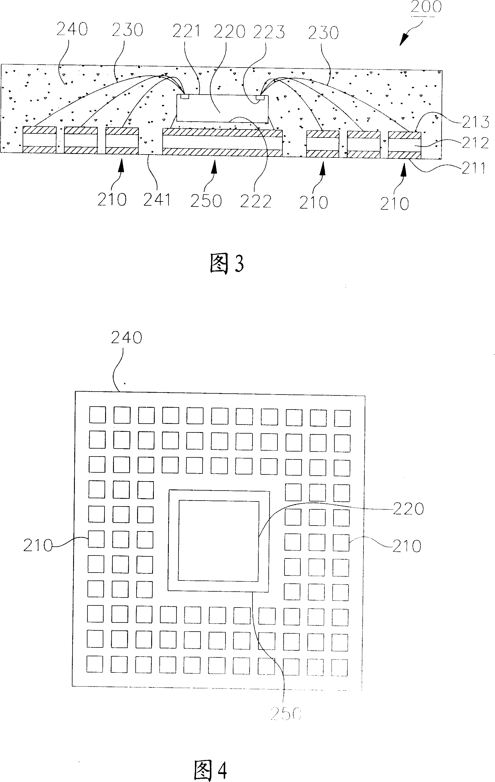
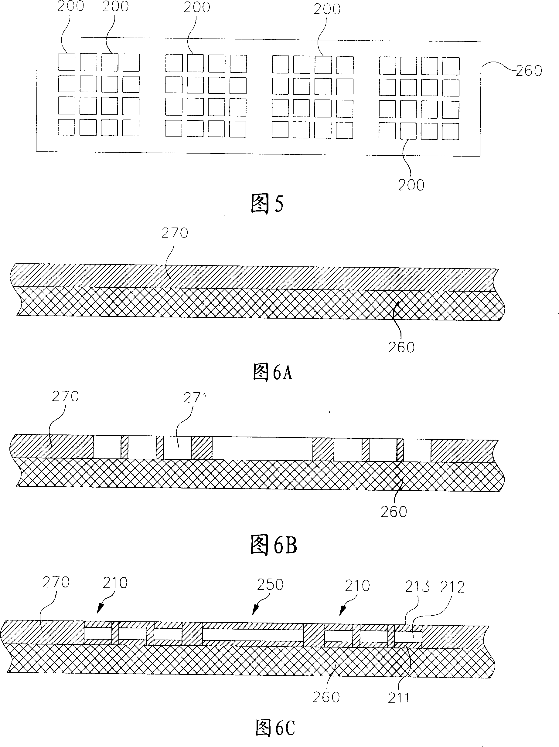
[0069] Please refer to FIG. 3 and FIG. 4. FIG. 3 is a schematic cross-sectional view of a chip package structure with array pads according to a first embodiment of the present invention. FIG. 4 is a chip and wire bonding structure of the chip package structure Schematic of the top surface of the pad. In the first embodiment of the present invention, the chip package structure 200 with array pads mainly includes a plurality of bonding pads 210 , a chip 220 , a plurality of bonding wires 230 and an encapsulant 240 .

[0070] As shown in FIG. 4 , the above-mentioned bonding pads 210 are arranged in an array, and can be arranged in any number of rows, which are formed by electroforming technology (details will be described later). Moreover, as shown in FIG. 3 , the bonding pads 210 are formed on the same plane. Each bonding pad 210 includes a lower bonding layer 211 , an electroformed core 212 and an upper bonding layer 213 , wherein:

[0071] The electroforming core 212 is made...

no. 3 Embodiment

[0093] Please refer to FIG. 9 , which is a schematic cross-sectional view of another chip package structure with array pads according to the third embodiment of the present invention. The present invention can be further applied to different chip package structures of non-wire bonding type. Another chip package structure 400 with array pads disclosed in the third embodiment mainly includes a plurality of pads 410, a chip 420 and A letter of colloid 430.

[0094] The pads 410 are formed in an array on the same plane. Each pad 410 includes a lower bonding layer 411 and an electroforming core 412, and may further include an upper bonding layer 413, so that the electroforming core 412 is located on the lower bonding layer. layer 411 and the upper bonding layer 413 .

[0095] The electroforming cores 412 are made of copper, which has the advantages of good thermal conductivity and easy electroforming. And the side surfaces 412A of the electroformed cores 412 are not covered by th...


PUM


Abstract

The present invention relates to a wafer packaging with array pads and its processing method. The wafer packaging mainly includes even numbers of wire-bonded pads, a wafer, even numbers of welding line and a sealing colloid. An upper and a lower combination layers are separately formed on cores of the wire-bonded pads, in which materials of the cores include copper. These welding lines electric connect the wafer with the upper combination layer of the wire-bonded pads. The sealing colloid seals these welding lines, cores and upper combination layers, in which only the lower combination layers are exposed out of the sealing colloid. The present invention can solve the former rusting problem of exposed cutting surface of pins in non-external-pin wafer packaging of conductor frame substrate, and has array pads which can achieve high density of wafer packaging. The processing method of the present invention keeps using a rigid conductive mold in packaging process to carry steps of electroforming, wafer attaching, wire bonding and packaging to achieve coherence of the packaging process.

Description

technical field [0001] The present invention relates to a packaging structure of a semiconductor chip, in particular to a packaging structure that can solve the problem of rusting on the exposed cutting surface of the pins in the conventional chip packaging structure without external pins on the lead frame base, and has an array of pads, which can achieve high density. Chip packaging, and continuous use of a rigid conductive template in the packaging process for electroforming, die bonding, wire bonding, and packaging steps, which can achieve consistent packaging operations. A chip packaging structure with array pads without external pins and its manufacturing method . Background technique [0002] In the prior known packaging technology, a lead frame base wafer package structure is a pinless type. The lower surface of the pin in the lead frame is bonded to the outer surface, replacing the outer pin of the conventional lead frame, and has the advantage of smaller surface fo...

Claims


Application Information

Patent Timeline
Patent Type & Authority Applications(China)
IPC IPC(8): H01L23/488H01L23/31H01L21/60H01L21/56
CPCH01L2224/92247H01L2224/484H01L24/48H01L2924/01046H01L2924/0105H01L2924/01082H01L2924/01047H01L2924/01079H01L2224/32245H01L2224/16H01L2224/48247H01L2924/01322H01L2924/01005H01L2924/01033H01L2924/01029H01L2224/13099H01L2924/01078H01L21/6835H01L2924/01028H01L24/16H01L2224/16245H01L2224/48091H01L2224/49171H01L2224/73265H01L24/73H01L2224/05554H01L2224/48H01L2924/181
Inventor 林鸿村
Owner CHIPMOS TECH INC
Why Eureka
Try Eureka