Ceramic packing member used for SMD crystal resonator and manufacturing technique thereof

A crystal resonator and ceramic packaging technology, which is applied in the direction of electric solid-state devices, semiconductor devices, semiconductor/solid-state device components, etc., can solve the problems of high production cost, complex product design, and numerous processes, and achieve simplified co-fired ceramics process , The effect of improving the electrical performance of the product and reducing the production cost

Inactive Publication Date: 2008-02-27
CHAOZHOU THREE CIRCLE GRP
View PDF1 Cites 24 Cited by
  • Summary
  • Abstract
  • Description
  • Claims
  • Application Information

AI Technical Summary

Problems solved by technology

[0003] The disadvantages of the existing crystal resonator ceramic packaging structure are: its product design and production process are complicated, and the production cost is high, which hinders the popularization and application of SMD ceramic packaging
[0007] The reasons are as follows: a. The ceramic layer is composed of a three-layer co-fired ceramic structure, the product design is complicated, the process is numerous, and the process cost is high; b. The structure of the cutting frame is adopted, and Ag / Cu solder needs to be brazed under the protection of the atmosphere. Soldering, high material and process costs; c. There are too many exposed metal parts, the area to be electroplated with gold is large, and the cost of gold plating is high; d. When using this package, the user must purchase a Kovar cover plate and use a parallel sealing welding process. Large equipment investment and high production cost

Method used


Image

  • Ceramic packing member used for SMD crystal resonator and manufacturing technique thereof
  • Ceramic packing member used for SMD crystal resonator and manufacturing technique thereof
  • Ceramic packing member used for SMD crystal resonator and manufacturing technique thereof

Examples


Embodiment Construction

[0042] With reference to Fig. 7 to Fig. 16, the present invention is implemented like this:

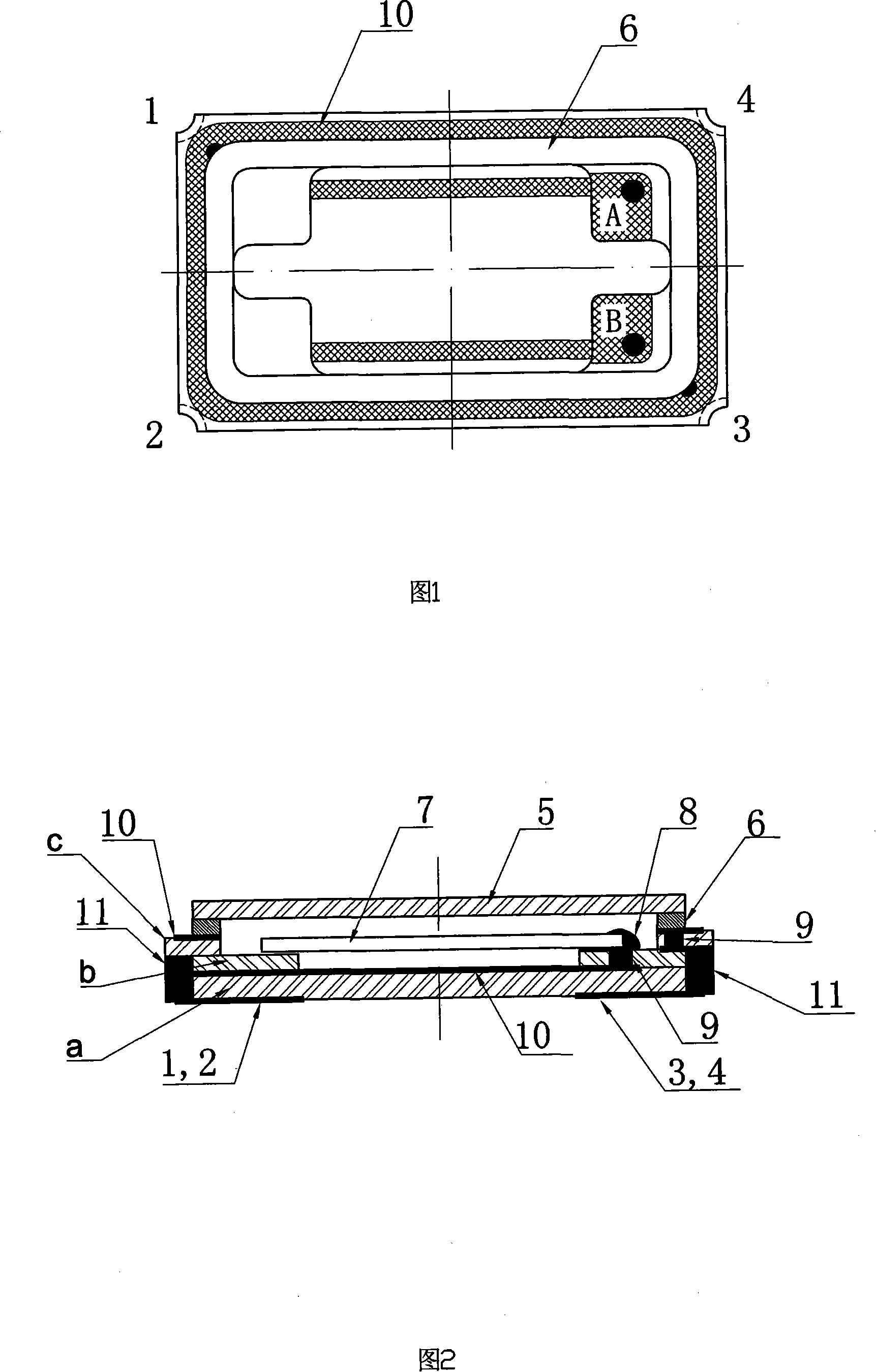
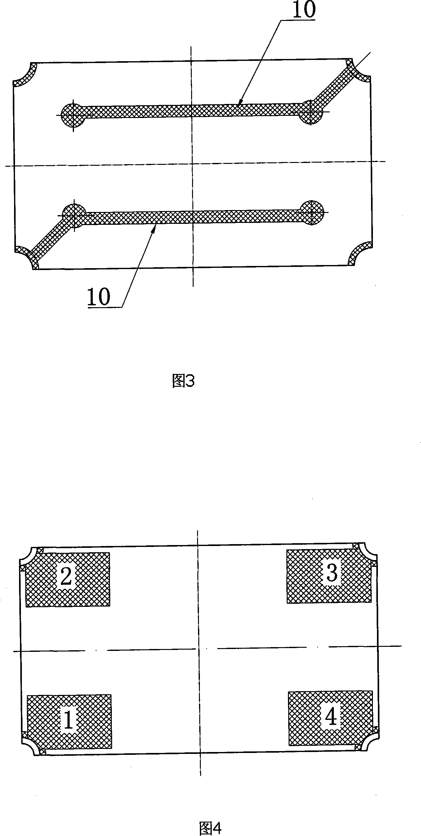
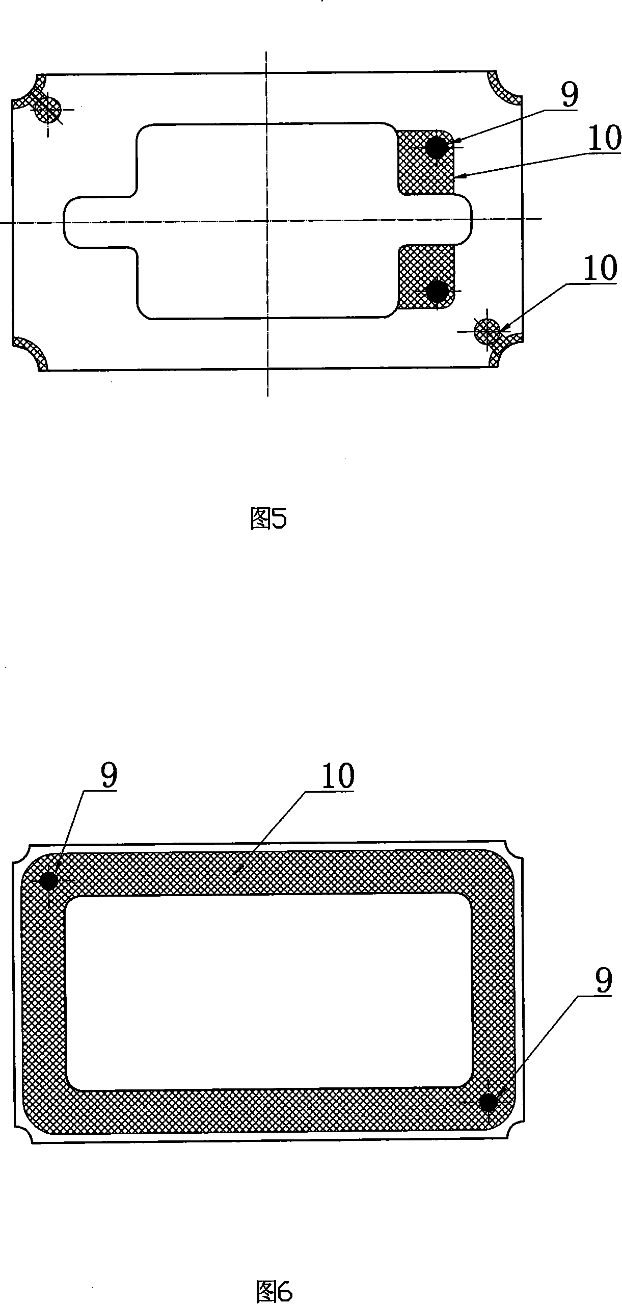
[0043] A ceramic package for SMD crystal resonators, comprising a bottom pad 1 and a bottom pad 2, a co-fired ceramic layer and a ceramic cover plate 3, and the co-fired ceramic layer is composed of a stacked first co-fired ceramic layer a Composed with the second co-fired ceramic layer b, a ceramic cover plate 3 is arranged on the top of the second co-fired ceramic layer b, and a printed support plate 3 is provided on the upper side of the first co-fired ceramic layer a. The electrodes on the resonant crystal 4 are connected to the pads on the bottom surface through the via holes on the first layer, and the bosses include a supporting boss C for supporting functions and two supporting conductive pads for conducting and supporting functions. The main function of the bosses A, B, and the supporting boss C is to provide a vibration space for the resonant crystal 4, and the outer periphe...


PUM


Abstract

This invention relates to a technique for ceramic packing the transistor resonator, particularly the ceramic package component used for SMD transistor resonator. It is composed of: the co-sintered ceramic layer and the ceramic cover. Said co-sintered ceramic layer comprises the coincided No.1 ceramic layer and No.2 ceramic layer. Over the No.2 layer is the ceramic cover; on the upper surface of the No.1 layer is the printed convex platform, which is used for supporting transistors and guiding the electrodes, through the holes, to the basal plane soldering plate. The advantages are: simple sintering process, low production cost, reducing shielding gas protective soldering, low kovar frame material requirement, low gold-plated area, and short leading wire.

Description

technical field [0001] The invention relates to a ceramic package technology for a crystal resonator, in particular to a ceramic package for an SMD crystal resonator and a production process thereof. Background technique [0002] At present, crystal resonators are mainly packaged in plastic and metal. Due to the requirements of surface mount technology (SMT) and miniaturization of electronic components, some high-end products with high reliability requirements use surface mount device (SMD) ceramic packages. The main factor for the promotion of SMD ceramic packaging is that the cost of ceramic packaging is too high, and the subsequent sealing process must use parallel sealing welding, which will make the equipment investment too large. The existing general crystal resonator structure is shown in Figure 1 to Figure 6, and its similar structure also has the Chinese patent No. ZL200520115009.3, the application date is August 2, 2005 "a ceramic package for crystal oscillator pi...

Claims


Application Information

Patent Timeline
Patent Type & Authority Applications(China)
IPC IPC(8): H03H9/02H03H9/10H03H3/02H01L23/02H01L25/00
Inventor 杨绍华
Owner CHAOZHOU THREE CIRCLE GRP
Why Eureka
Try Eureka