Method for enhancing upside-down mounting welding core plate brightness
A flip-chip, chip technology, applied in electrical components, electrical solid-state devices, circuits, etc., can solve the problems of less reflection and high absorptivity
Inactive Publication Date: 2008-03-12
上海蓝宝光电材料有限公司
View PDF0 Cites 10 Cited by
- Summary
- Abstract
- Description
- Claims
- Application Information
AI Technical Summary
Problems solved by technology
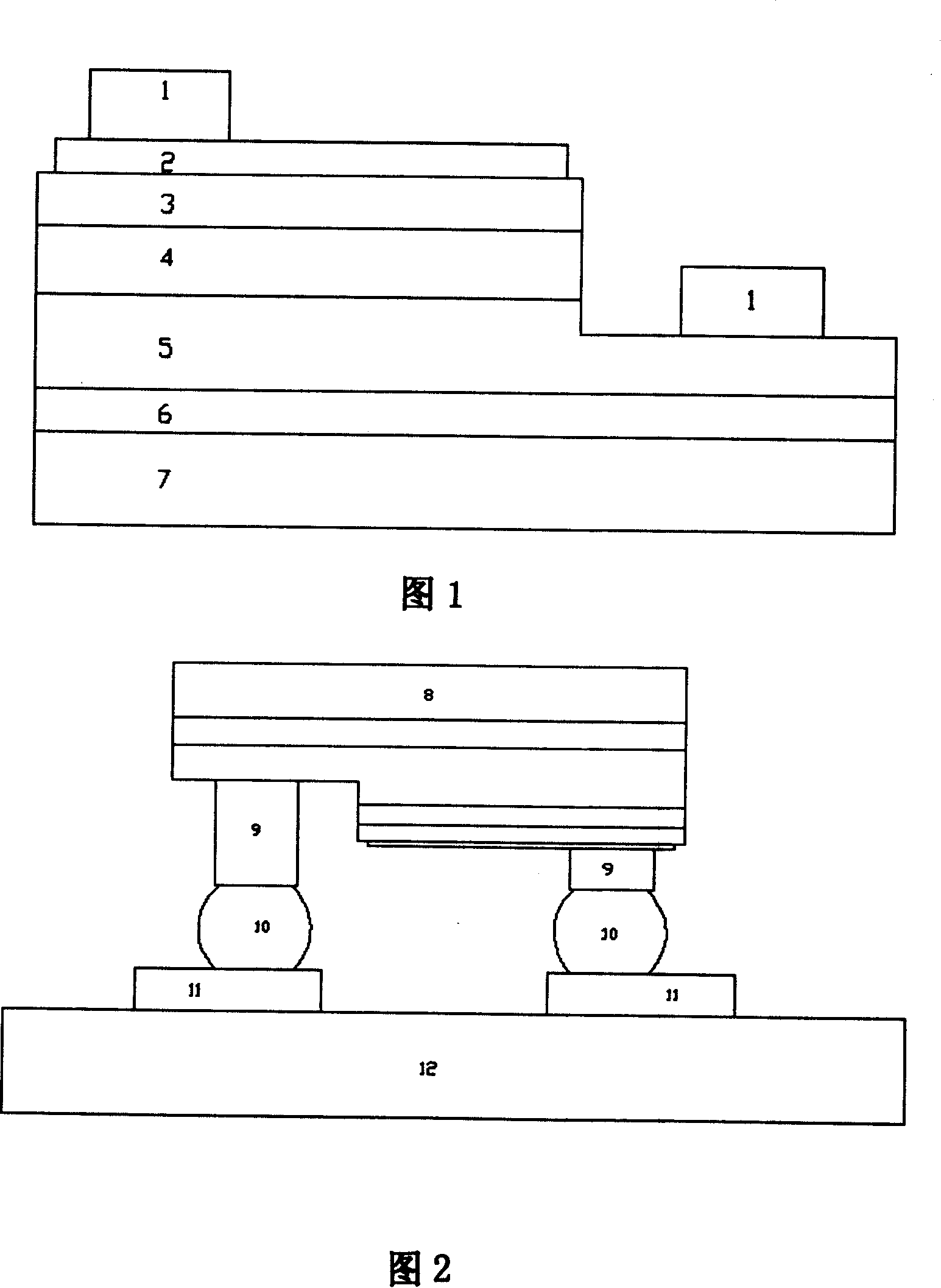
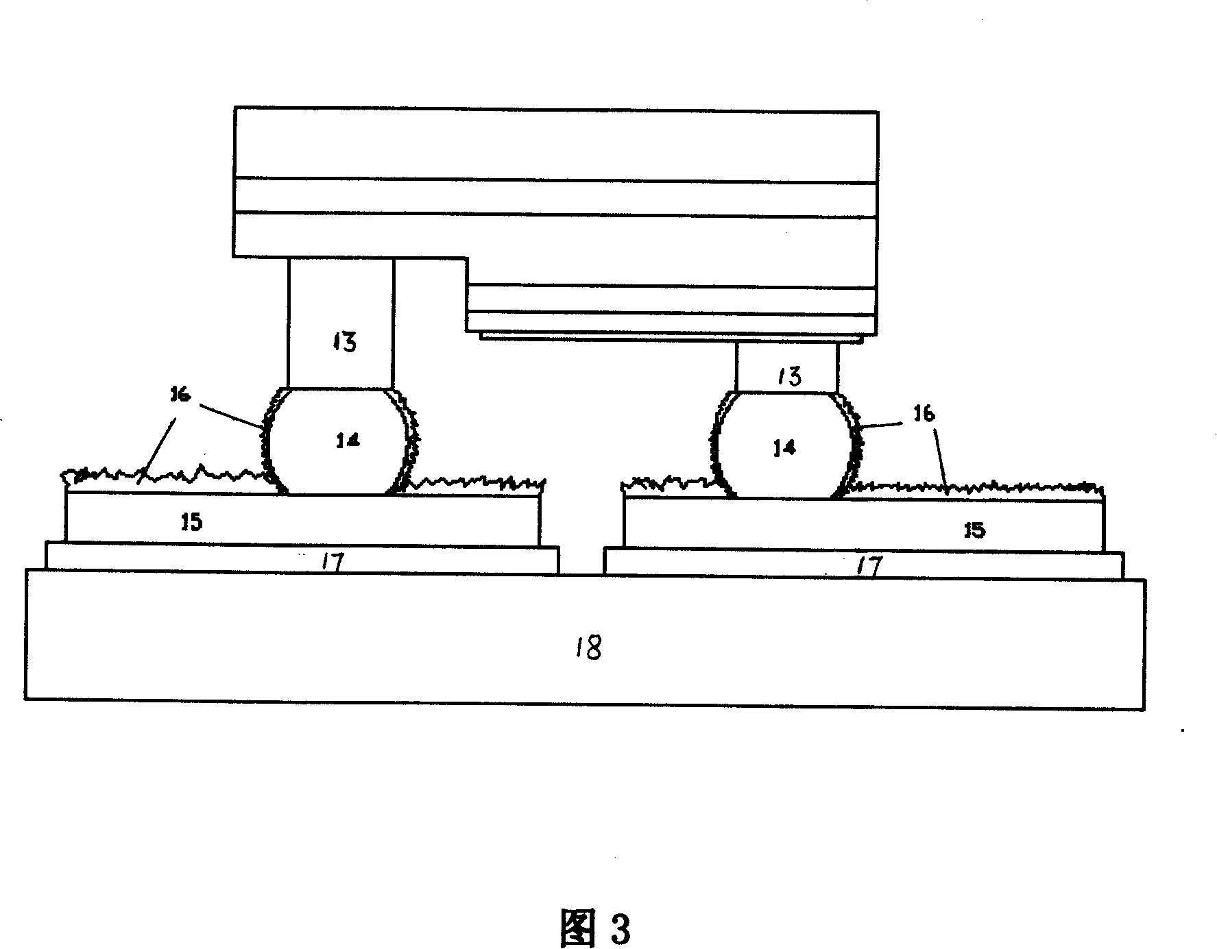
However, since the metal circuit 11 on the silicon heat sink substrate 12 accounts for a small proportion of the surface area of the silicon heat sink substrate 12, and also has a high absorption rate of light, when the light shines on the silicon heat sink substrate 12, most of the The light is absorbed by the silicon heat sink substrate 12 with little reflection; in addition, the metal balls 10 used for the combination of the flip chip and the silicon heat sink substrate are gold balls, which themselves absorb a lot of light, thus causing the present flip chip Luminous efficiency is only ~301m / W
Method used
View moreImage
Smart ImageViewing Examples

Examples
Embodiment 2
[0019] On the two positive and negative metals 15 and gold balls 14, a layer of 3 μm thick high-reflectivity metal aluminum layer was plated on the two pieces of positive and negative metals 15 and gold balls 14 respectively, and the others were the same as in Example 1.
Login to View More PUM
 Abstract
The invention relates to a method for lighting up the backbonded chip, which is characterized in plating the metal of high reflectivity onto the original metal circuit and the light absorbed golden ball. The method is: first, oxidizing the silicon substrate with heat reacting furnace to generate a silicon dioxide layer, photoetching the pattern by photo exposure machine and etching the needless silicon dioxide with hydrofluoric acid buffer solution of 1% to 3%, vapor depositing a layer of high reflectivity metal onto the silicon dioxide layer by thermal coater and etching two adjacent positive and negative electrodes which covers 40% to 95% surface areas of the silicon substrate ferric nitrate mixed solution; second, balling the golden balls on the surface of both positive and negative electrodes by balling machine, plating a layer of high reflectivity metal respectively on two positive and negative electrodes and the golden balls by thermal coater, etching the high reflectivity metal layer with hydrofluoric acid buffer solution and the left metal layer is adhered to two positive and negative electrodes and the golden balls; finally, converting the chip by wire bonder to make its electrodes aligned with the golden balls, and compaginating the electrodes with golden balls by heating and ultra audible sound. The invention has the advantage of increasing the optical efficiency of 40% more than that of traditional backbonded chip.
Description
technical field [0001] The invention relates to a method for improving the brightness of a flip-chip welding chip, in particular to a method for increasing the reflection of light by plating metal on a supporting substrate of the flip-chip, thereby improving the brightness of the chip, which belongs to the technical field of LEDs. Background technique [0002] The so-called light-emitting diode (LED) is a P / N diode made of a semiconductor material with a direct energy gap. Under the condition of thermal equilibrium, most of the electrons do not have enough energy to jump to the conduction band. When forward bias is applied, the electrons will jump to the conduction band, and the original position of the electrons on the original bond band will generate holes. Under proper bias voltage, electrons and holes will combine in the P / N interface area (P-N Juction) to emit light, and the current of the power supply will continuously replenish electrons and holes to N-type semiconduc...
Claims
Login to View More Application Information
Patent Timeline
 Patent Type & Authority Applications(China)
IPC IPC(8): H01L33/00H01L21/60
CPCH01L2224/16225
Inventor 冯雅清叶国光应华兵章加奇
Owner 上海蓝宝光电材料有限公司