Ground wire layout graph for reducing microwave single-sheet integrated circuit standing wave ratio

An integrated circuit and microwave monolithic technology, applied to circuits, printed circuits, waveguides, etc., to facilitate installation and adjustment, improve success rate, and reduce process errors

Inactive Publication Date: 2008-03-19
INST OF MICROELECTRONICS CHINESE ACAD OF SCI
View PDF0 Cites 6 Cited by
  • Summary
  • Abstract
  • Description
  • Claims
  • Application Information

AI Technical Summary

Problems solved by technology

The circuit simulation found that the coplanar waveguide has a great influence on the input and output standing wave ratio, but since the SMA test head added at the

Method used


Image

  • Ground wire layout graph for reducing microwave single-sheet integrated circuit standing wave ratio
  • Ground wire layout graph for reducing microwave single-sheet integrated circuit standing wave ratio
  • Ground wire layout graph for reducing microwave single-sheet integrated circuit standing wave ratio

Examples


Example Embodiment

[0040] Example

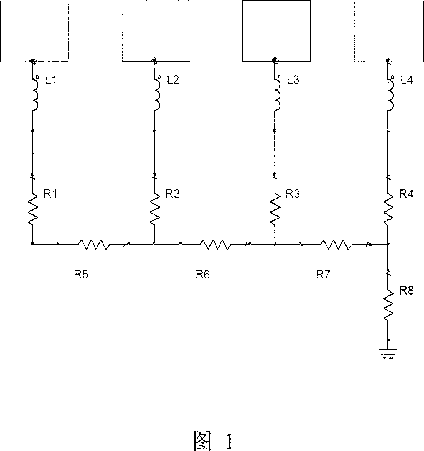
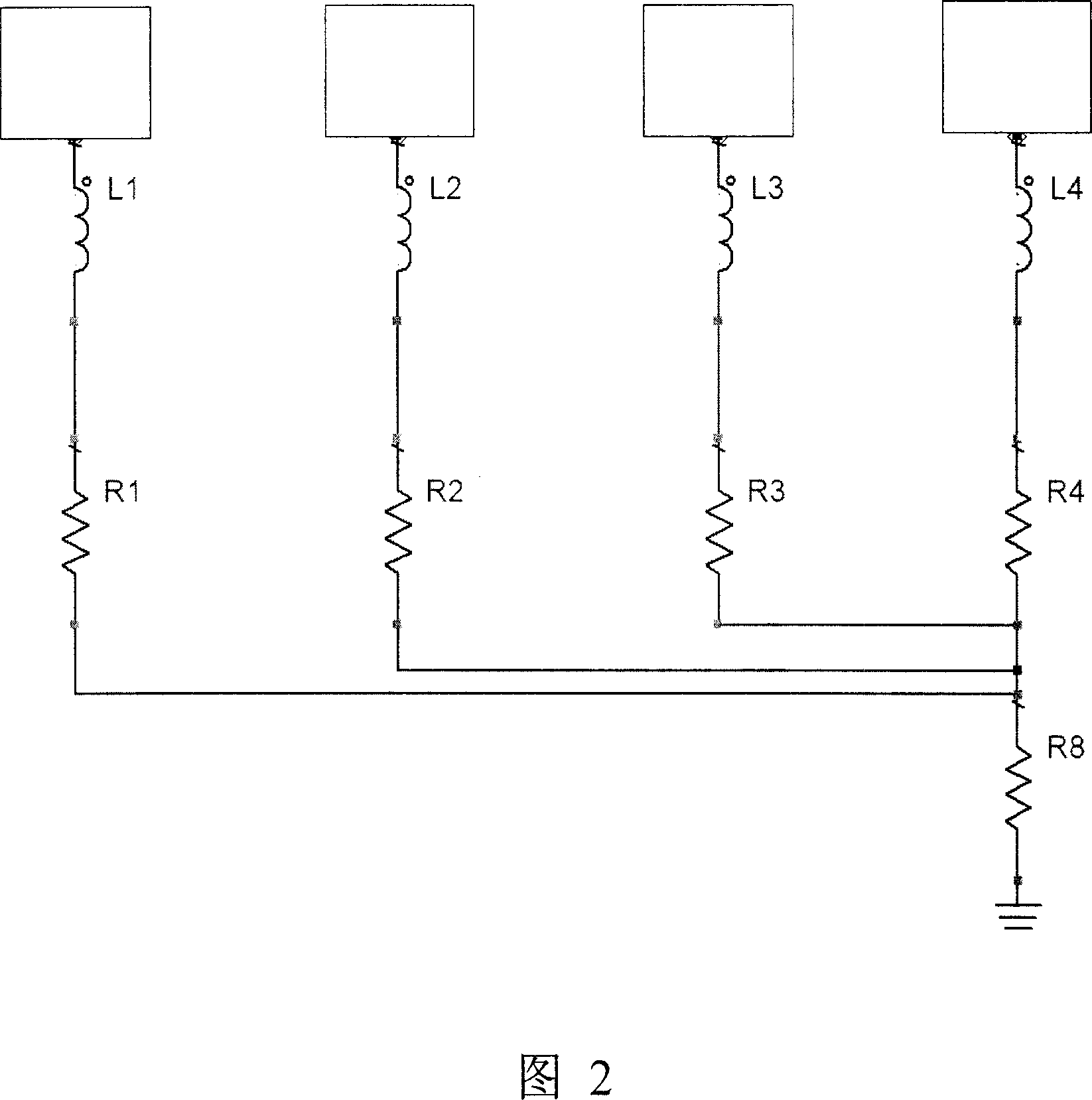
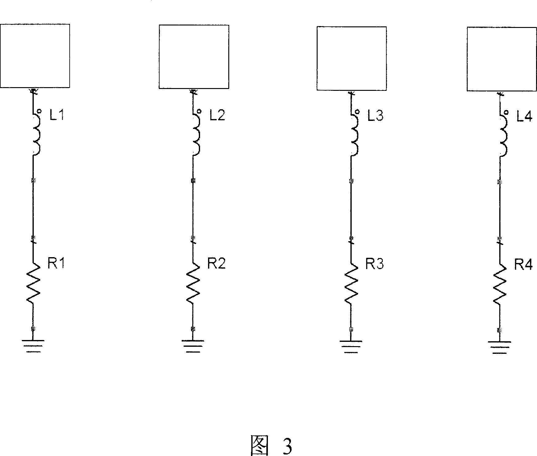
[0041] As shown in FIG. 5, FIG. 5 is a ground wire layout pattern for reducing the MMIC standing wave ratio according to a preferred embodiment of the present invention. Figure 5 shows the ground layout of the input part and the output part.

[0042] The graphic unit is located on the same layer of the printed circuit board or layout. The printed circuit board does not use a solder resist layer and maintains the gold surface. This is because the skin effect of the current in the high-frequency circuit requires a smooth gold surface. If a solder mask is added, the gold surface will not have a polishing process, so the solder mask is not used. The width of the signal microstrip is determined by the center frequency point. The distance between the signal microstrip and the ground plane is calculated according to the coplanar waveguide formula. The distance between the device under test (DUT) is calculated by the microstrip line, and the value is 2-3 times the width o...


PUM


Abstract

The invention discloses a ground wiring pattern for reducing the standing-wave ratio of a microwave monolithic integrated circuit (MMIC), which is characterized in that the ground wiring pattern at least comprises a pattern unit, wherein the pattern unit is composed of a signal microstrip line which is printed on a printed circuit board and a domain plane and which has a Z-shaped projecting pattern, and earth wire grounded through holes distributed along the signal microstrip line. The invention can reduce the increase in standing-wave ratio caused by the inductance of metal jumper wire and the processing error of capacitance blocking capacitor, and facilitate the installation of the elements required for the regulation of standing-wave ratio, without inducing large parasitic inductance. Therefore, the invention can reduce the mismatched sensitivity of input/output terminals to the change of imaginary impedance, improve the standing-wave ratio, and increase the success rate of MMIC test.

Description

Technical field [0001] The invention relates to the technical field of printed circuit board (PCB) or layout (layout) wiring, in particular to a ground wire layout pattern for reducing the standing wave ratio of a microwave monolithic integrated circuit (MMIC). Background technique [0002] As the feature size of the large-scale integrated circuit becomes smaller and smaller, the parasitic capacitance, parasitic inductance, and resistance in the printed circuit board (PCB) or layout (layout) have an increasingly greater impact on the performance of the integrated circuit. [0003] Although in an ideal situation, the ground plane should be at an equipotential ground plane with a potential of 0, but due to the parasitic capacitance and parasitic inductance in the printed circuit board (PCB) or layout (layout) ground wire layout, , The influence of resistance, poor ground wire layout, or when the ground wire is far away from the device under test (DUT), will produce a lot of electro...

Claims


Application Information

Patent Timeline
IPC IPC(8): H01L23/48H01L23/66H01P3/08H05K1/00
CPCH01L2924/3011H01L2224/49175H01L2924/30107
Inventor 朱旻张海英
Owner INST OF MICROELECTRONICS CHINESE ACAD OF SCI
Why Eureka
Try Eureka