

Semiconductor luminescent device and mfg method thereof
A light-emitting device and manufacturing method technology, applied in semiconductor devices, electrical components, circuits, etc., can solve the problems of difficulty in growing GaN, poor crystal integrity, and low doping efficiency of P-type GaN, so as to improve the effect of current expansion and eliminate current Blocking effect, the effect of simple and easy process
- Summary
- Abstract
- Description
- Claims
- Application Information
AI Technical Summary
Problems solved by technology
Method used
Image

Examples
Embodiment 1
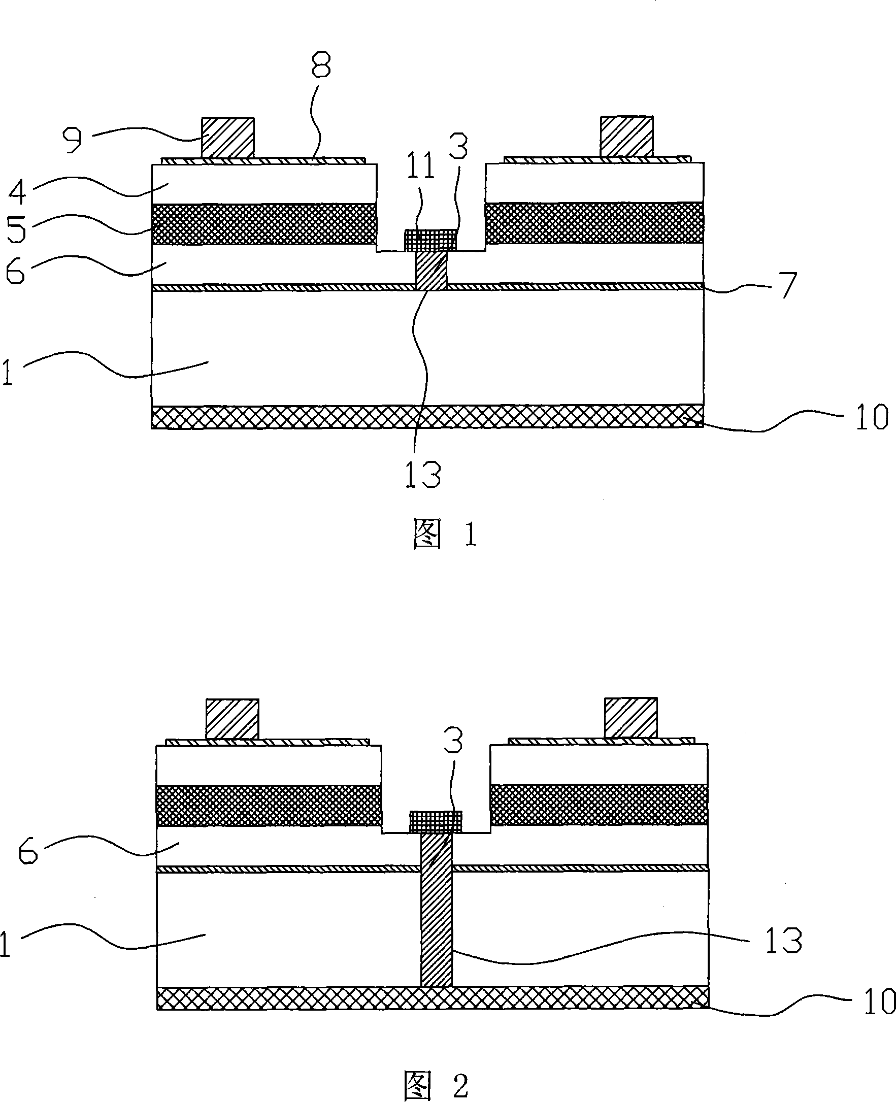
[0026] With reference to Fig. 1, a kind of semiconductor light-emitting device, it comprises substrate 1 and the semiconductor epitaxial laminated layer stacked on substrate 1, and this semiconductor epitaxial laminated layer comprises N-type layer 6, light-emitting layer 5 and P-type layer successively from bottom to top. Layer 4, a layer of transparent conductive film 8 is formed on the upper surface of the P-type layer 4, a P-type electrode 9 is arranged on the transparent conductive film 8, and an electrode 10 is arranged on the lower surface of the substrate 1, wherein the N-type layer 6 A conductor is provided inside, one end of which exposes the N-type layer 6 , and an N-type electrode 11 is provided, the other end of which is in electrical contact with the substrate 1 .
[0027] The conductor is composed of a columnar through hole 13 and a conductive substance 3 filled in the through hole 13 . The through hole 13 is a columnar through hole with a circular or square cro...
Embodiment 2
[0043] As shown in Figure 2, this embodiment is similar to Embodiment 1, the difference is that in this embodiment, in order to reduce the internal resistance of the substrate 1, the through hole 13 can be etched through the entire substrate 1 to form a full through hole. , and the conductive substance 3 is filled in the through hole 13, and the N-type layer 6 is directly in electrical contact with the electrode 10 at the lower end of the substrate 1 through the conductive substance 3.
[0044] Of course, according to different requirements on the internal resistance of the semiconductor light emitting device in practical applications, the through hole 13 may also partially penetrate the substrate 1 .
Embodiment 3
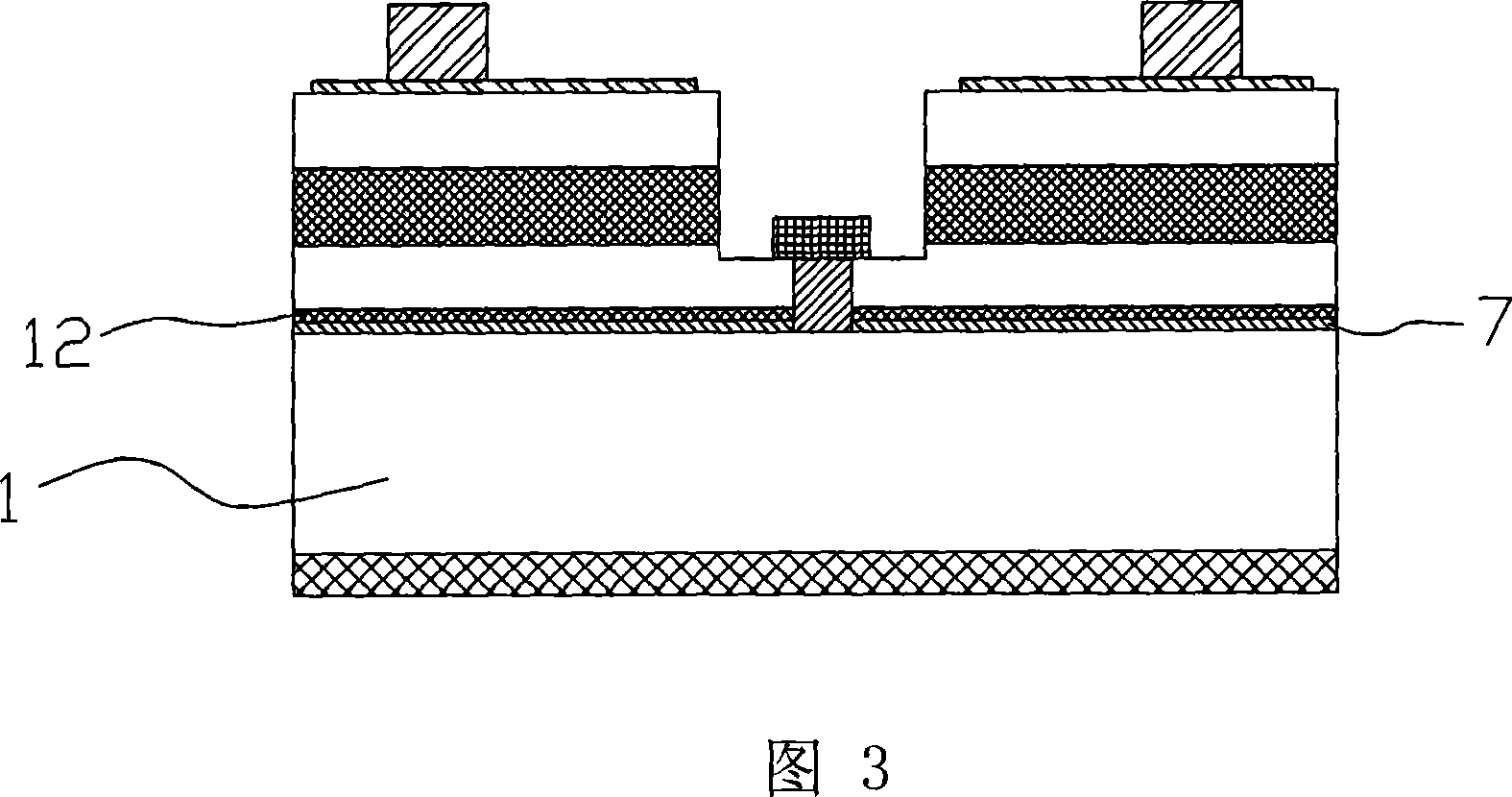
[0046] As shown in Figure 3, this embodiment is similar to Embodiment 1, and the difference is that in this embodiment, in order to improve the light extraction efficiency of the semiconductor light emitting device, aluminum gallium indium nitrogen (InxGayAl1-x -yN, 0<=x<=1, 0<=y<=1) DBR reflective layer 12 of material (typical structure is AlGaN / AlN etc.), at this moment through hole 13 structures need to be etched during dry process Etching passes through the DBR reflective layer 12 and the buffer layer 7 to reach the substrate 1 .
[0047] Of course, according to different requirements on the internal resistance of the semiconductor light emitting device in practical applications, the through hole 13 may partially or completely penetrate the substrate 1 by using a method similar to that of Embodiment 2.
PUM
 Abstract
Description
Claims
Application Information