

Method for producing two-dimensional polymer photon crystal using flexible offset printing
A technology of lithography and photonic crystals, which is applied in the field of soft lithography to produce two-dimensional polymer photonic crystals, can solve the problems of low modulus of PDMS templates, and achieve high fidelity and high production capacity
- Summary
- Abstract
- Description
- Claims
- Application Information
AI Technical Summary
Problems solved by technology
Method used
Image

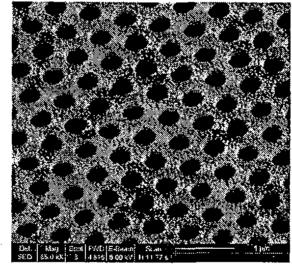
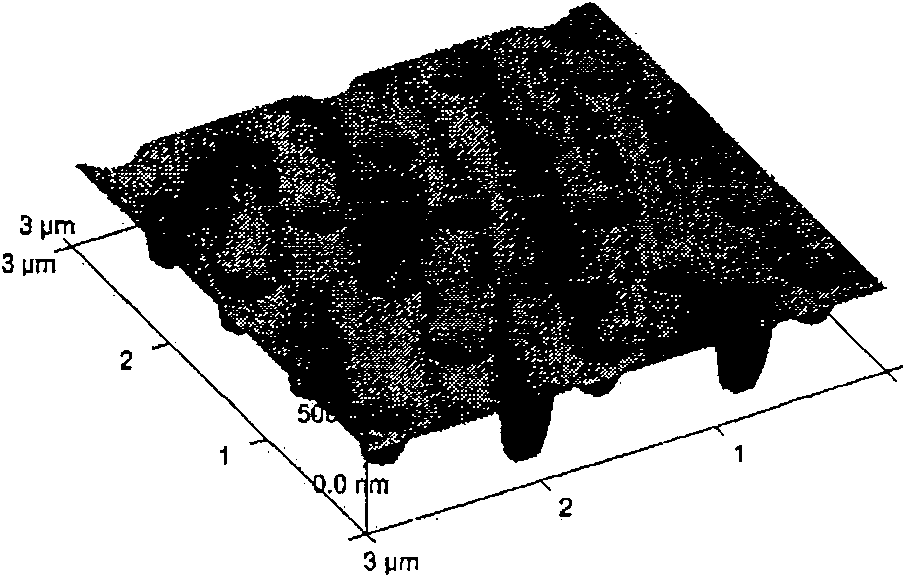
Examples
Embodiment 1
[0032] Example 1: Fabrication of two-dimensional ultraviolet acrylic polymer photonic crystals.
[0033] Materials used in the examples are as follows:
[0034] The ultraviolet acrylic polymer model WIR30-470 is produced and sold by ChemOptics, Korea.
[0035] The electronic etchant is ZEP520A, produced and sold by Japan ZEON Company.
[0036] ZED-N50 solvent: developer for electronic etching adhesive ZEP520A, produced and sold by Japan ZEON Company.
[0037] The PDMS model is Sylgard 184, with a specific gravity of 1.11 and a viscosity of 5000cSt, produced and sold by Dow Corning.
[0038] Proceed as follows:
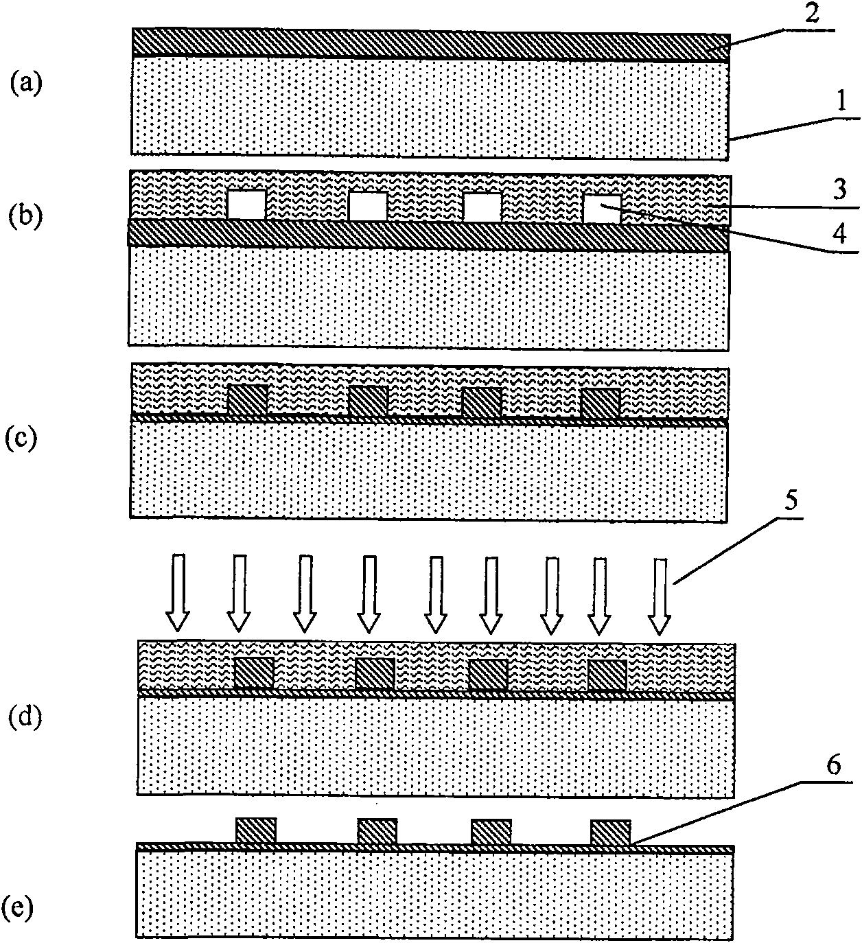
[0039] (1) Substrate fabrication of triangular cavity structure
[0040] Using JEOL JBX6000 electron beam lithography (EBL) equipment, a layer of electronic etching glue (ER) ZEP520A is coated on the silicon substrate, the pattern is determined and printed by EBL, and the exposed electronic etching glue is in ZED-N50 solvent After development, bake on a baking tray ...
PUM
| Property | Measurement | Unit |
|---|---|---|
| diameter | aaaaa | aaaaa |
| tackiness | aaaaa | aaaaa |
| depth | aaaaa | aaaaa |
Abstract
Description
Claims
Application Information