Aligning system and lightscribing device using the system

An alignment system and alignment mark technology, which is applied in the field of alignment technology and lithography equipment, can solve problems such as occupancy, multi-line slot area, and large mark size, and achieve cost reduction, signal-to-noise ratio improvement, and high sensitivity Effect

Active Publication Date: 2010-04-14
SHANGHAI MICRO ELECTRONICS EQUIP (GRP) CO LTD
View PDF7 Cites 0 Cited by
  • Summary
  • Abstract
  • Description
  • Claims
  • Application Information

AI Technical Summary

Problems solved by technology

However, the high-order diffraction light enhanced alignment marks SPM-AH32, SPM-AH53, and SPM-AH74 with periodic subdivision structures can only enhance the light intensity of one high-order diffraction order at the same time, although VSPM marks can Simultaneously achieve 3rd, 5th and 7th order diffracted light enhancement, but the size of the mark is too large, occupying more area of ​​the marking groove

Method used


Image

  • Aligning system and lightscribing device using the system
  • Aligning system and lightscribing device using the system
  • Aligning system and lightscribing device using the system

Examples


Embodiment Construction

[0033] The specific embodiments of the present invention will be further described below in conjunction with the accompanying drawings.

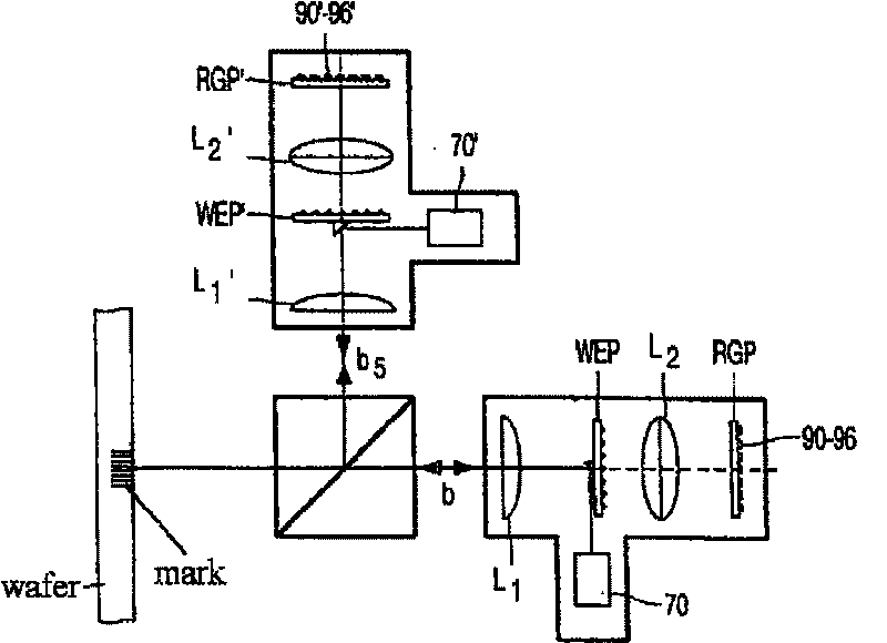
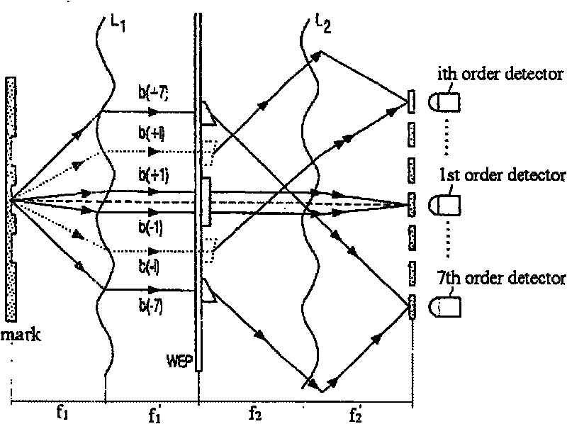
[0034] Figure 1(a) to Figure 1(g) A schematic diagram of a prior art dual-laser multi-level diffraction grating off-axis alignment (ATHENA) alignment system is shown. Among them, Fig. 1(a) shows the structure diagram of the prior art dual-laser multi-level diffraction grating off-axis alignment (ATHENA) alignment system, and Fig. 1(b) shows the prior art dual-laser multi-level diffraction Schematic diagram of the grating off-axis alignment (ATHENA) alignment system. The alignment system adopts red light 70 and green light 70' double laser light sources in the light source; the optical system structure is 4f system, and the wedge array or wedge plate group WEP and WEP' located on the spectrum plane is used to achieve alignment Separation of different orders of diffracted light marked, respectively coherent imaging on the image plane; throu...


PUM


Abstract

After the modulation of reference grating, the light intemsity variation of diffracted light coherent imaging in +-1 stage of the alignment mark is detected at image surface; meanwhile at the pupil surface, the variation of interference signal intensity in each stage being coherent and stacking with the positive, negative diffracted light spot in same stage with the high stage diffracted light ofthe alignment light is detected. The generated signals have high process versatility, high sensitivity and high S / N ratio.

Description

technical field [0001] The invention relates to photolithography devices in the field of integrated circuit or other micro-device manufacturing, in particular to an alignment technology and photolithography devices. Background technique [0002] Lithography equipment is mainly used in the manufacture of integrated circuits IC or other micro-devices. Through a photolithographic apparatus, multilayer masks with different mask patterns are sequentially imaged on a photoresist-coated wafer under precise alignment. There are currently two types of photolithography devices, one is a stepper photolithography device, the mask pattern is exposed and imaged on one exposure area of ​​the wafer, and then the wafer moves relative to the reticle to move the next exposure area to the mask pattern and projection Below the objective lens, the mask pattern is again exposed on another exposed area of ​​the wafer, and the process is repeated until all exposed areas on the wafer have an image o...

Claims


Application Information

Patent Timeline
Patent Type & Authority Patents(China)
IPC IPC(8): G03F7/20G03F7/207G03F9/00
Inventor 徐荣伟
Owner SHANGHAI MICRO ELECTRONICS EQUIP (GRP) CO LTD
Why Eureka
Try Eureka