Silicon thin-film solar cell and manufacturing method therefor

A solar cell and manufacturing method technology, applied in semiconductor/solid-state device manufacturing, circuits, photovoltaic power generation, etc., can solve the problems of low battery utilization rate, complex packaging process, poor bonding force between the packaging layer and the battery body, etc., to improve the weather resistance. performance and stability, simple packaging process, and the effect of meeting different requirements

Active Publication Date: 2008-05-14
李毅
View PDF2 Cites 36 Cited by
  • Summary
  • Abstract
  • Description
  • Claims
  • Application Information

AI Technical Summary

Problems solved by technology

[0007] Therefore, the current thin-film solar cells have the following problems: 1. When used outdoors, the weather resistance and stability of the product are still insufficient; The area utilization rate of the effective thin-film battery is low, and it is difficult to match the output voltage and current of the battery; 3. The traditional packaging process is complicated, inconvenient to operate, and the bonding force between the packaging layer and the battery body is poor

Method used


Image

  • Silicon thin-film solar cell and manufacturing method therefor
  • Silicon thin-film solar cell and manufacturing method therefor
  • Silicon thin-film solar cell and manufacturing method therefor

Examples


Embodiment 1

[0043] Example 1: Production of a small strong-light single-junction amorphous silicon solar cell with an outline of 50mm×50mm×3.0mm and a pitch of 10mm.

[0044] A silicon thin-film solar cell with a shape of 50mm×50mm×3.0mm is composed of 5 unit nodes with a pitch of 10mm. The process steps are as follows:

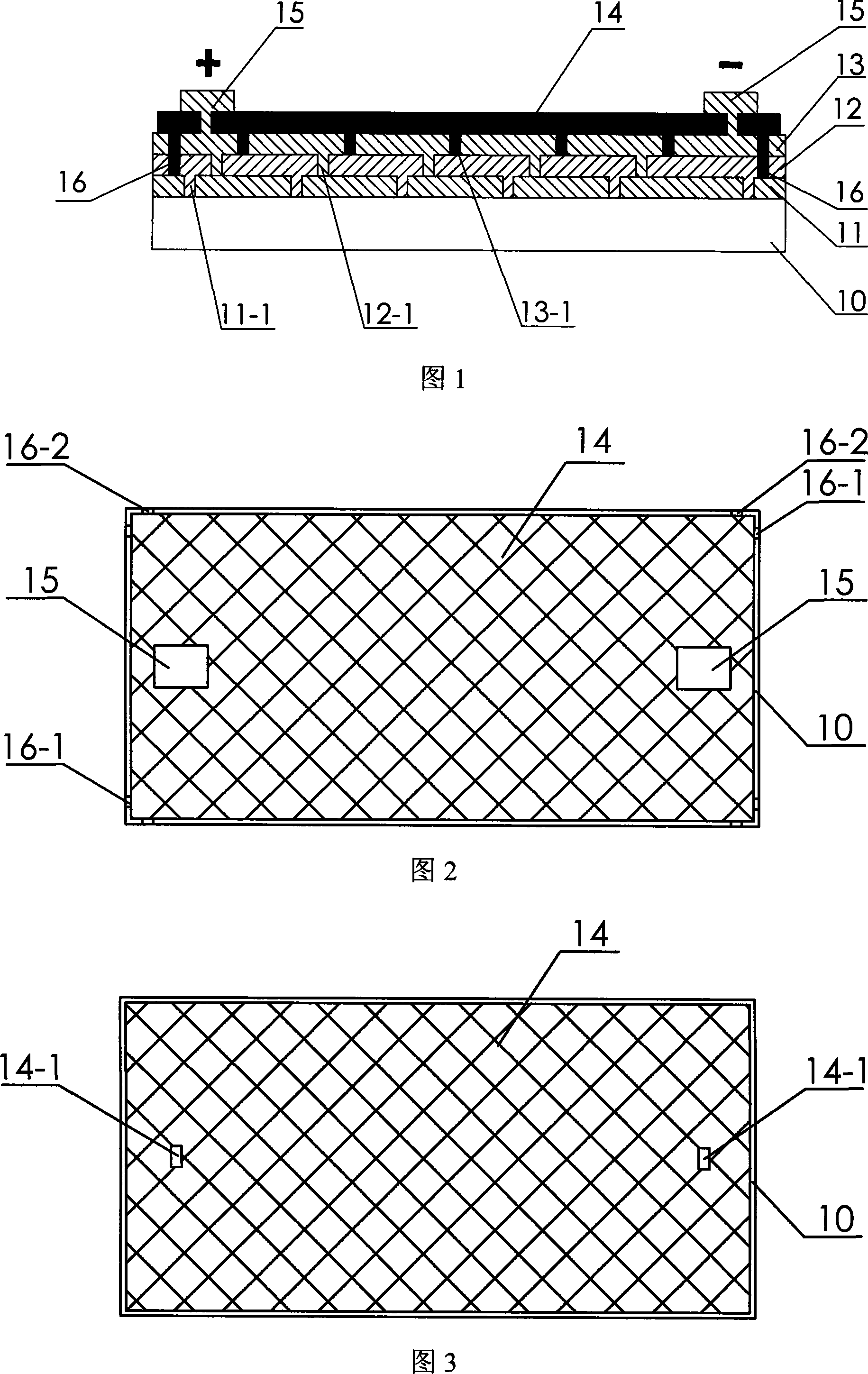
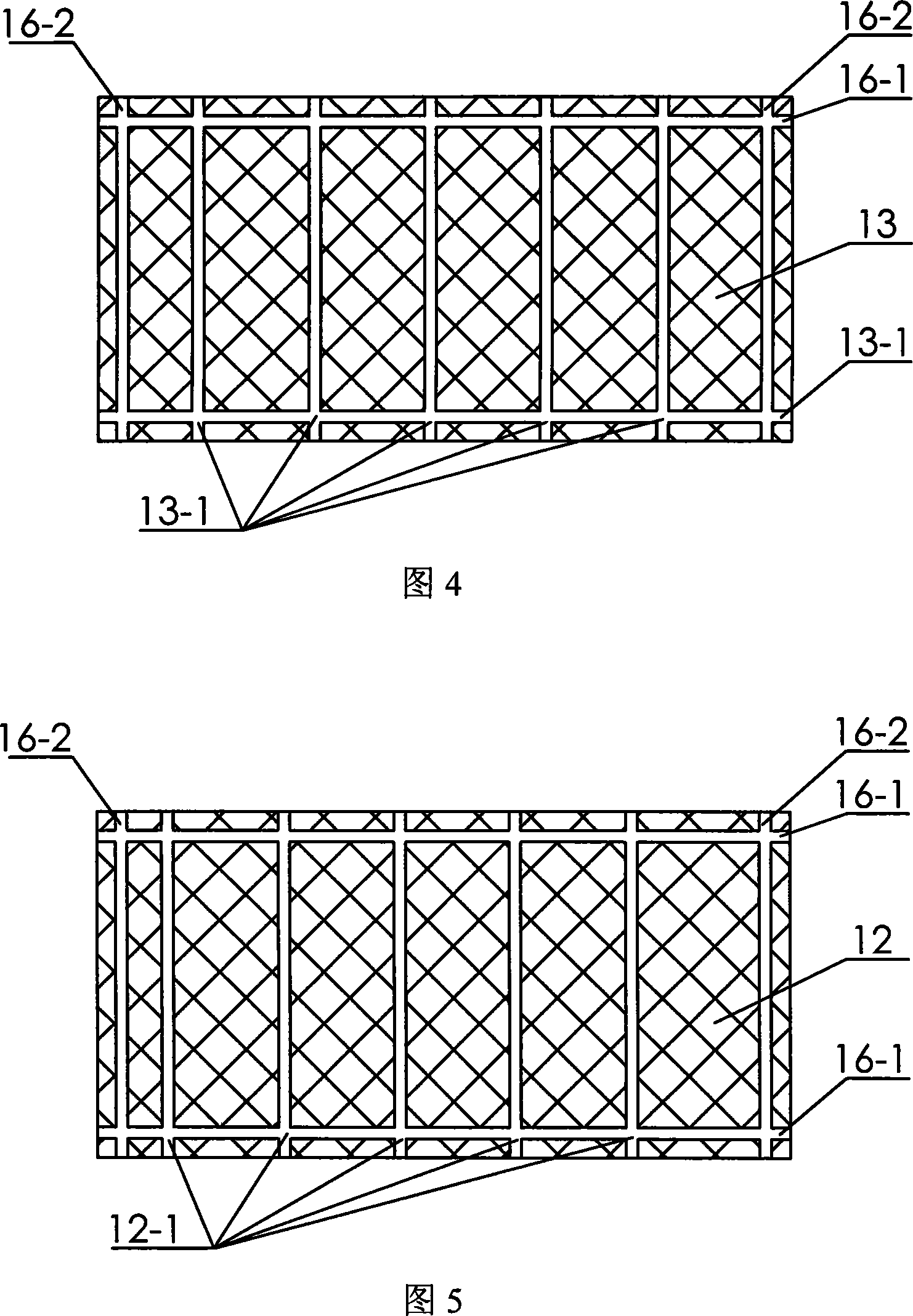
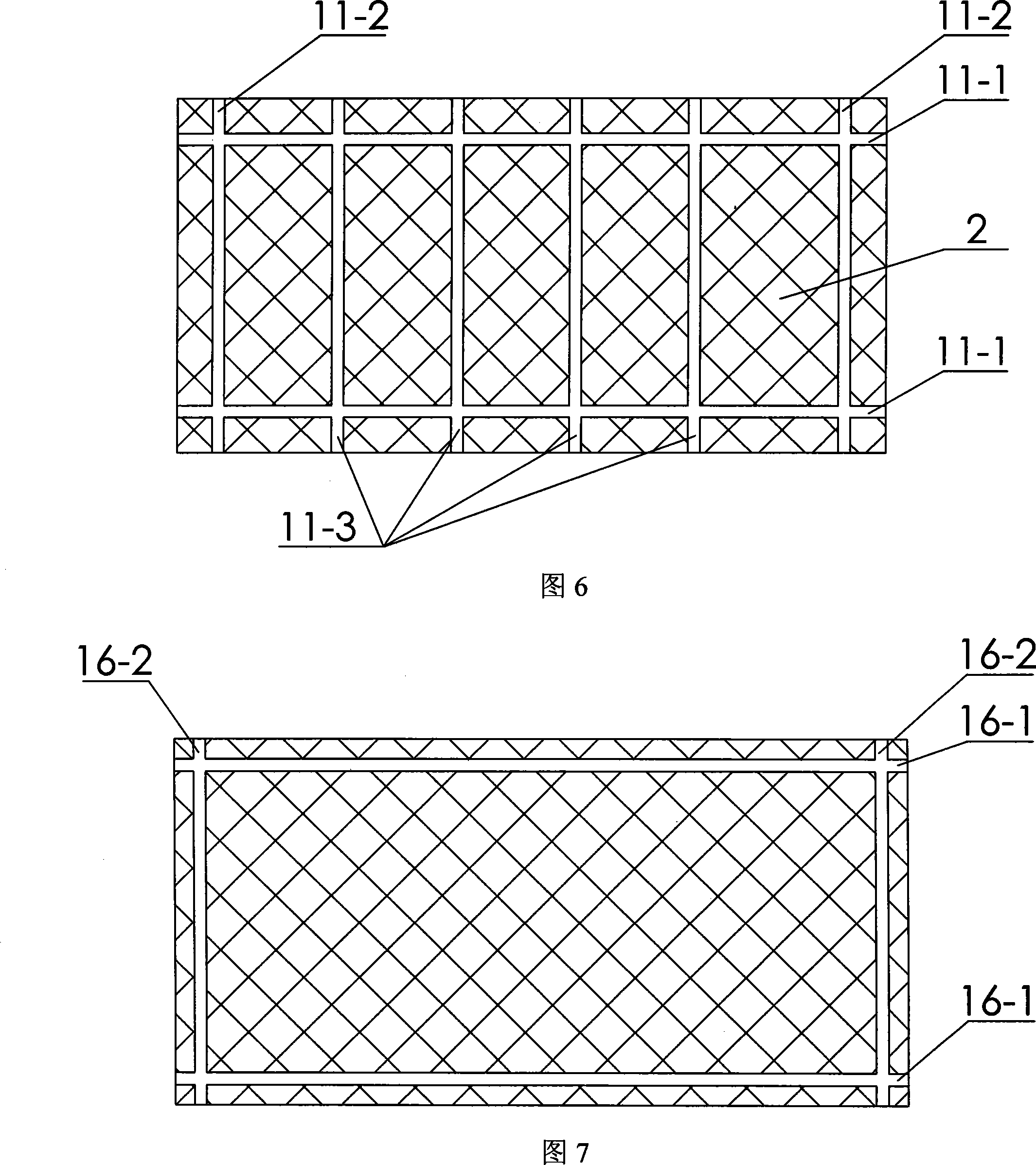
[0045] Step 1, front electrode 11 graphic production: use ITO or SnO with an array pitch of 50mm×50mm according to the design 2 The transparent conductive film glass is used as the substrate, and the continuous conductive film on the substrate is etched into independent small pieces with a spacing of 10mm by laser. Transverse groove; 11-2 is the longitudinal groove of the front electrode film layer; 11-3 is the segmented groove of the front electrode film layer, which constitutes the front electrode pattern.

[0046] Step 2. Deposit thin film battery layer 12: After the substrate with the front electrode pattern engraved is ultrasonically cleaned and dried, preheated, a...

example 2

[0055] Example 2: Production of small strong light double-junction amorphous silicon solar cells with a shape of 60mm×60mm×3.0mm and a pitch of 12mm.

[0056] A silicon thin-film solar cell with a shape of 60mm×60mm×3.0mm is composed of 6 unit nodes with a pitch of 12mm. The process steps are as follows:

[0057] Step 1. Fabrication of front electrode 11 pattern: use ITO or SnO 2 The transparent conductive film glass is used as the substrate. Lasers are used to etch the continuous conductive film on the substrate into independent small blocks with a spacing of 12 mm. The small blocks are insulated from each other, as shown in the shaded part in Figure 6, which is the front electrode pattern.

[0058] Step 2. Depositing the double-junction amorphous silicon layer 12: After the substrate with the engraved front electrode pattern is ultrasonically cleaned and dried, preheated, and the top cell P is sequentially deposited on the substrate by plasma chemical vapor deposition (PECVD...

Embodiment 3

[0067] Example 3: Production of laminated thin-film solar cells with an outline of 350 mm×1220 mm×3.0 mm and a pitch of 20 mm.

[0068] Proceed as follows:

[0069] Step 1. Fabrication of the front electrode pattern: ITO or SnO with a size of 350mm×1220mm 2 The transparent conductive film glass is used as the substrate, and the continuous conductive film on the substrate is etched into independent small blocks with a spacing of 20 mm by laser scribing. The small blocks are insulated from each other, that is, the front electrode pattern.

[0070] Step 2. Deposition of the top cell: After ultrasonic cleaning and drying of the substrate with the engraved front electrode pattern, preheating, and the enhanced plasma chemical vapor deposition (PECVD) method is used to sequentially deposit P-type amorphous silicon on the substrate. Layer, I-type intrinsic amorphous silicon layer and N-type amorphous silicon doped layer, and lasers are used to engrave the corresponding position in th...


PUM


Abstract

The invention relates a thin film silicon solar cell and the manufacturing method thereof; the thin film silicon solar cell is widely applied to the energy-saving electronic products such as the lawn lambs, the yard lambs, etc. The thin film silicon solar cell consists of the large-scale integrated tandem type cell units, uses a transparent conducting basal-plate as the substrate, and comprises a front electrode layer, a thin film cell layer, a back electrode layer and a back layer which are sequentially superposed; the elementary cell consisting of the tandem type cell units is provided with an insulation groove etched by the laser around the cell, and a screen-printed back paint layer within the groove having the performances of insulation, welding resistance, moisture resistance, and acid and alkali resistance. The thin film silicon solar cell provided by the invention can not only prevent the short circuit and the leakage current around the cell, but also prevent the moisture in the air from entering the cell with causing the deliquescence.

Description

Technical field [0001] The invention provides a silicon thin-film solar cell and a manufacturing method thereof, and relates to a silicon thin-film solar cell and a manufacturing method thereof that are widely used in energy-saving electronic products such as lawn lamps and garden lights. Background technique [0002] As we all know, for solar cells, thin-film batteries are the second generation of solar cells. Due to the rich source of raw materials, no pollution, low energy consumption, and low production costs, they are green and environmentally friendly products. Since the 21st century, thin-film batteries have developed rapidly. With the continuous advancement of thin-film solar cell technology, the cost performance of the product is reasonable, and there are more and more uses. [0003] The traditional manufacturing method of thin-film solar cells, as shown in Figure 10, is to deposit a front electrode layer 3 on a transparent conductive substrate 2, etch a channel 6 w...

Claims


Application Information

Patent Timeline
Patent Type & Authority Applications(China)
IPC IPC(8): H01L27/142H01L21/82H01L31/046
CPCY02E10/50
Inventor 李毅李全相
Owner 李毅
Why Eureka
Try Eureka