

Gallium nitride based LED epitaxial slice structure and method for preparing the same
A light-emitting diode, gallium nitride-based technology, applied in the direction of electrical components, circuits, semiconductor devices, etc., can solve the problem of low light extraction efficiency, achieve the effect of improving luminous efficiency, improving light extraction efficiency, and improving performance
- Summary
- Abstract
- Description
- Claims
- Application Information
AI Technical Summary
Problems solved by technology
Method used
Image

Examples
Embodiment 1
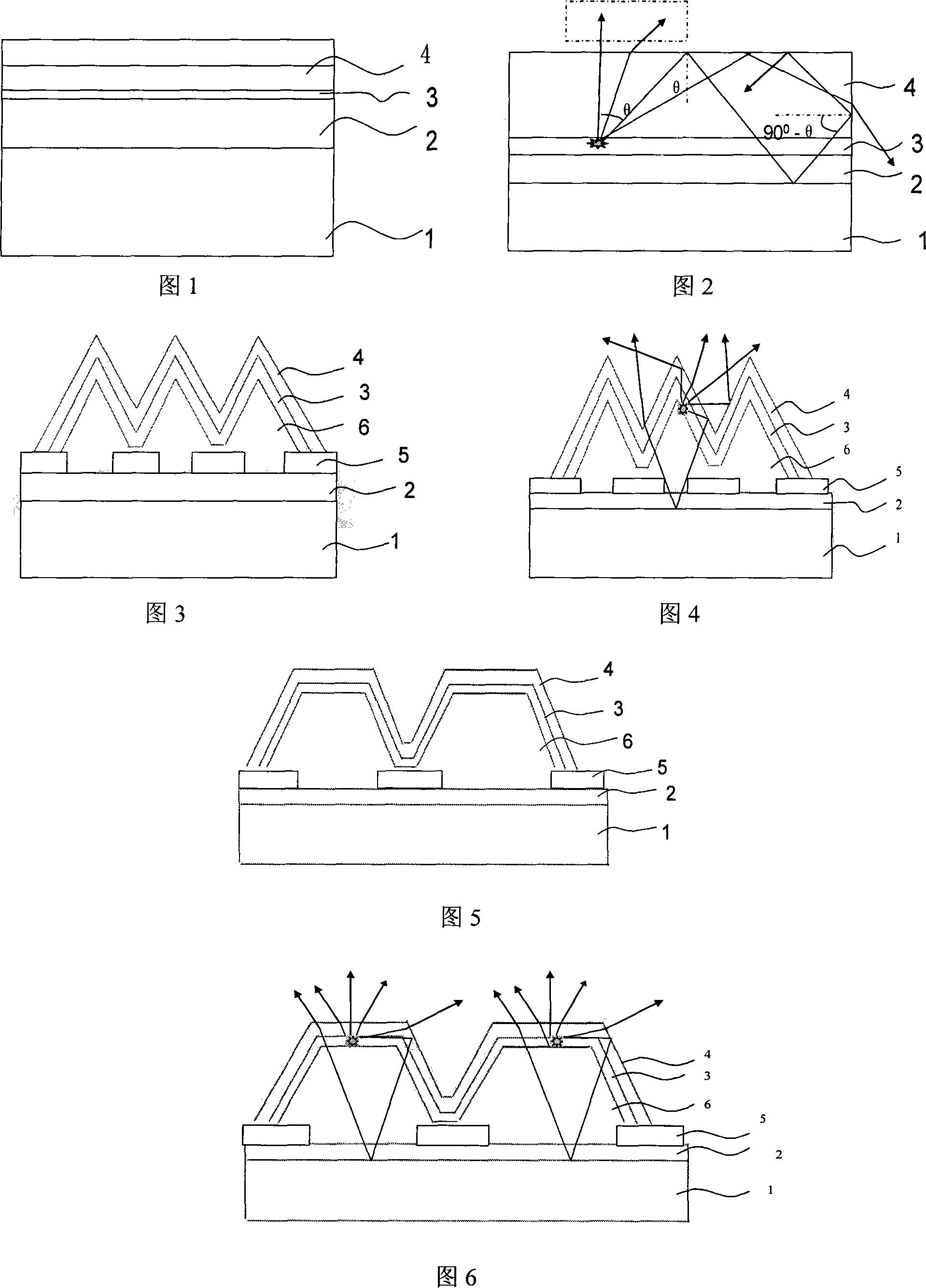
[0035] Referring to Fig. 3, the GaN-based light-emitting diode epitaxial wafer structure according to the present invention is provided with a sapphire substrate 1, an undoped GaN buffer layer (not shown in Fig. 3), the first silicon-doped GaN layer 2, Dielectric layer 5, second silicon-doped GaN layer 6, 3 to 5 cycles of InGaN / GaN multiple quantum wells 3, magnesium-doped AlGaN layer and magnesium-doped GaN layer 4, undoped GaN buffer layer from bottom to top, the first Silicon-doped GaN layer 2, dielectric layer 5, second silicon-doped GaN layer 6, InGaN / GaN multiple quantum wells 7 of 3 to 5 periods, magnesium-doped AlGaN layer and magnesium-doped GaN layer 4 are sequentially arranged on sapphire substrate 1 ; The thickness of the undoped GaN buffer layer is 10-40 nm, the thickness of the first silicon-doped GaN layer is 2-3 μm, the thickness of the dielectric layer is 100-200 nm, and the thickness of the second silicon-doped GaN layer is 2-3 μm, The thickness of each cycle...
Embodiment 2
[0045] (1) Load the (0001) orientation no-clean sapphire substrate into the reaction chamber, and 2 Under atmosphere, heat to 1080°C and bake for 10 minutes, and the pressure in the reaction chamber is 500 Torr.
[0046] (2) Grow a GaN buffer layer with a thickness of 30nm at 530°C, the growth pressure is 500Torr, the flow rate of TMGa is 50μmol / min, NH3 The flow rate is 150 μmol / min.
[0047] (3) The GaN layer and the first silicon-doped GaN layer are grown at 1050° C., and the growth pressures are 200 Torr and 100 Torr respectively.
[0048] (4) Depositing SiO by PE-CVD at 300°C 2 layer, with a thickness of 200nm, etched along the silicon-doped GaN layer by conventional photolithography The direction carves out window areas of different shapes and sizes.
[0049] (5) Clean the patterned sample and put it into the metal organic chemical vapor deposition system (MOCV system) for epitaxial growth (secondary epitaxy).
[0050] (6) Secondary epitaxy: first in H 2 The second...
Embodiment 3
[0053] (1) Load the (0001) orientation no-clean sapphire substrate into the reaction chamber, and 2 Under atmosphere, heat to 1060°C and bake for 15 minutes, and the pressure in the reaction chamber is 500 Torr.
[0054] (2) Grow a GaN buffer layer with a thickness of 25nm at 550°C, the growth pressure is 500Torr, the flow rate of TMGa is 65μmol / min, NH 3 The flow rate is 180 μmol / min.
[0055] (3) The GaN layer and the first silicon-doped GaN layer are grown at 1030° C., and the growth pressures are 200 Torr and 100 Torr, respectively.
[0056] (4) Depositing SiO by PE-CVD at 300°C 2 , with a thickness of 150nm, along the n-GaN Window areas of different shapes and sizes are engraved in different directions.
[0057] (5) Clean the patterned sample and put it into the metal organic chemical vapor deposition system (MOCV system) for epitaxial growth (secondary epitaxy)
[0058] (6) Secondary epitaxy: first in H 2 The second silicon-doped GaN layer was grown under atmosphe...
PUM
| Property | Measurement | Unit |
|---|---|---|
| Thickness | aaaaa | aaaaa |
| Thickness | aaaaa | aaaaa |
| Thickness | aaaaa | aaaaa |
Abstract
Description
Claims
Application Information