Electric control optical switch array micro-fluidic chip manufacture method

A technology of microfluidic chips and optical switch arrays, applied in the coupling of optical waveguides, optics, optical components, etc., can solve the problems of limited switching capacity of optical switches, difficulty in making large arrays, etc., and achieve high speed performance, high Efficiency characteristics, effect of large switching capacity

Inactive Publication Date: 2008-05-28
NANJING UNIV OF POSTS & TELECOMM
View PDF0 Cites 23 Cited by
  • Summary
  • Abstract
  • Description
  • Claims
  • Application Information

AI Technical Summary

Problems solved by technology

[0004] Although the existing optical switches have their own unique advantages, it also allows us to see the shortcomings of the existing optical switches, especially the parameter of the switching matrix.
Except for a few types of optical switches such as MEMS, the switching capacity of existing optical switches is always limited, and it is difficult to make a large array; and MEMS optical switches themselves are also insufficient in terms of high port density and resistance to mechanical friction, wear or vibration. place

Method used


Image

  • Electric control optical switch array micro-fluidic chip manufacture method
  • Electric control optical switch array micro-fluidic chip manufacture method

Examples


Embodiment Construction

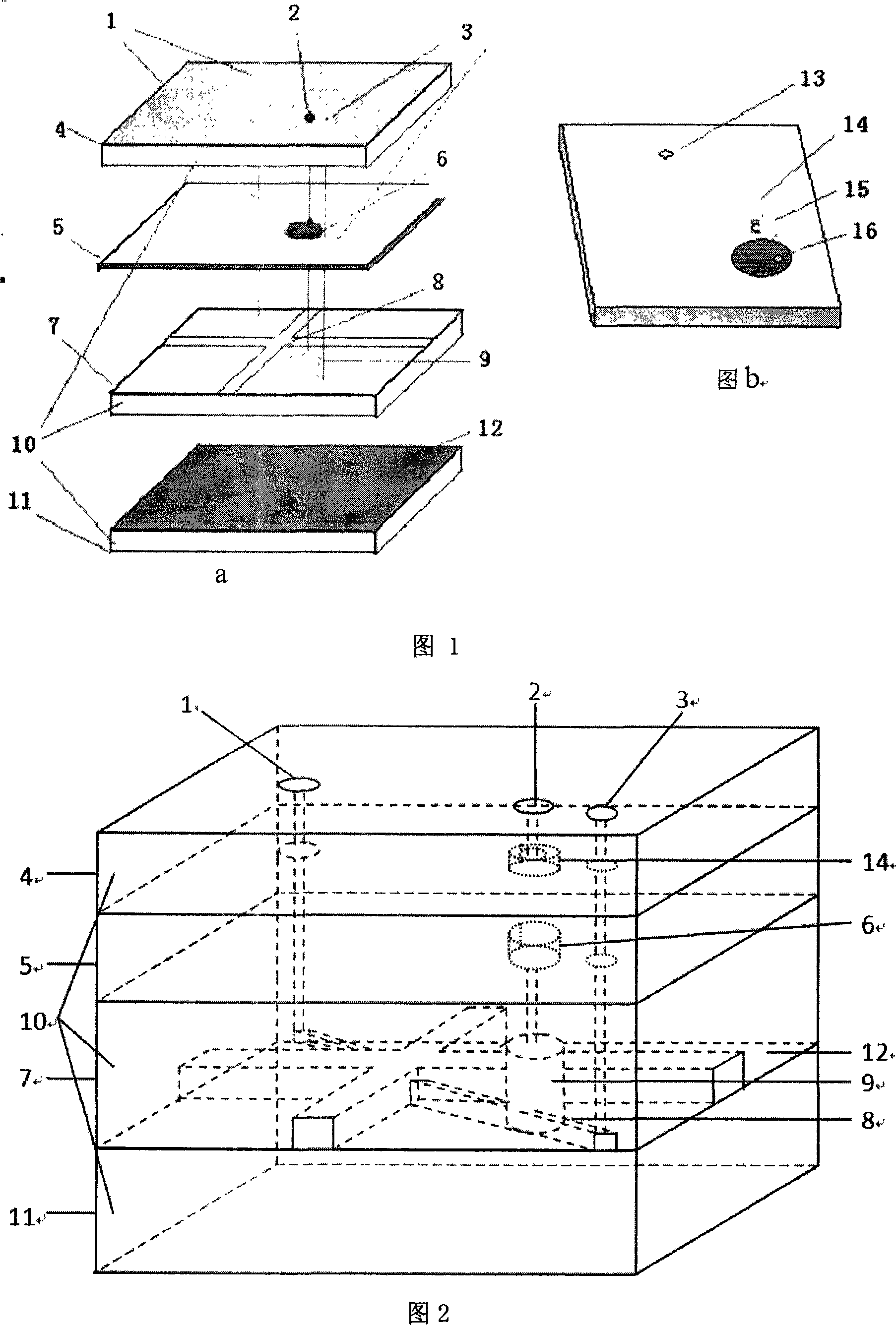
[0038]The invention proposes an array optical switch structure based on microfluidic technology, which adopts a sandwich structure of "optical waveguide layer + bottom conductive layer + insulating layer with conductive film block + upper cover plate". Wherein, the substrates of the cover plate, the optical waveguide layer and the bottom plate are polydimethylsiloxane (PDMS). PDMS has good light transmission, dielectric properties, inertness, non-toxicity, easy processing and other properties, and is cheap; the liquid in the micro-channels, thin tubes and liquid storage tanks on the optical waveguide layer is 201# methyl silicone oil. 201# methyl silicone oil has the characteristics of small temperature viscosity coefficient, high and low temperature resistance, anti-oxidation, high flash point, low volatility, good insulation, low surface tension, no corrosion to metal, and non-toxic; the insulating layer material is Polyvinyl alcohol (PVA) film. PVA film has good toughness,...


PUM


Abstract

The invention discloses a method for producing micro flow control optical switch array processes and relates to a novel integral producing method for an optical switch array frame which is operated through electric control signals. The novel integral producing method is based on a micro flow control technique. The method adopts mechanical processing, PDMS micro flow control chip production, coating, and sealing to realize integral production of a sandwich frame which includes 'a light wave guiding layer (7), a base plate conducting layer (11), an insulating layer (5) with a conducting film block, and an upper cover plate (4)' and realize the frame of micro flow control optical switch array chip. Main steps of the integral producing method comprise: production of the light wave guiding layer, production of a driving switch frame, production of the base plate conducting layer, and chip sealing, wherein basal material of a cover plate, the light wave guiding layer, and the base plate is polydimethyl siloxane (PDMS), and the conducting film block on the insulating layer are produced through adopting PVA thin films.

Description

technical field [0001] The invention relates to a novel integrated manufacturing method of an electrically tuned microfluidic control optical switch array chip, and belongs to the technical field of optical communication network device integration. Background technique [0002] Microfluidic optics is a new technology of great significance. It combines modern microfluidic technology and micro-optoelectronics technology to develop a class of optical integrated devices and The system will have important application prospects in the fields of sensing, communication, and information processing. [0003] As the key and core of micro-total analysis system, microfluidic technology has always been a research focus in the field of MEMS. With the continuous improvement of the level of microfluidic technology and the continuous penetration and integration with other disciplines, a number of eye-catching research hotspots have emerged in recent years, among which microfluidic optical de...

Claims


Application Information

Patent Timeline
Patent Type & Authority Applications(China)
IPC IPC(8): G02B6/35G02B26/02
Inventor 涂兴华徐宁梁忠诚沈鹏李培培陈金秋
Owner NANJING UNIV OF POSTS & TELECOMM
Why Eureka
Try Eureka