Semiconductor laser light source for emitting nanometer dimension vertical to cavity surface and method for making

A vertical cavity surface emission, nanoscale technology, applied in the direction of semiconductor lasers, lasers, laser components, etc., can solve the problems of difficult measurement and control, complex devices with high resolution in the near field or high storage density, and achieve threshold current Low density, good for integration, and small size

Inactive Publication Date: 2008-06-18
INST OF SEMICONDUCTORS - CHINESE ACAD OF SCI
View PDF0 Cites 10 Cited by
  • Summary
  • Abstract
  • Description
  • Claims
  • Application Information

AI Technical Summary

Problems solved by technology

[0005] However, ordinary VASL lasers can only obtain a super-diffraction-resolved spot size better than 1 / 2 wavelength within a distance of 100 nanometers in the near field, and the measurement and control of the 100-nanometer distance is difficult to achieve in optical memory applications. Devices with near-field high resolution or high storage density are too complex

Method used


Image

  • Semiconductor laser light source for emitting nanometer dimension vertical to cavity surface and method for making
  • Semiconductor laser light source for emitting nanometer dimension vertical to cavity surface and method for making
  • Semiconductor laser light source for emitting nanometer dimension vertical to cavity surface and method for making

Examples


Embodiment Construction

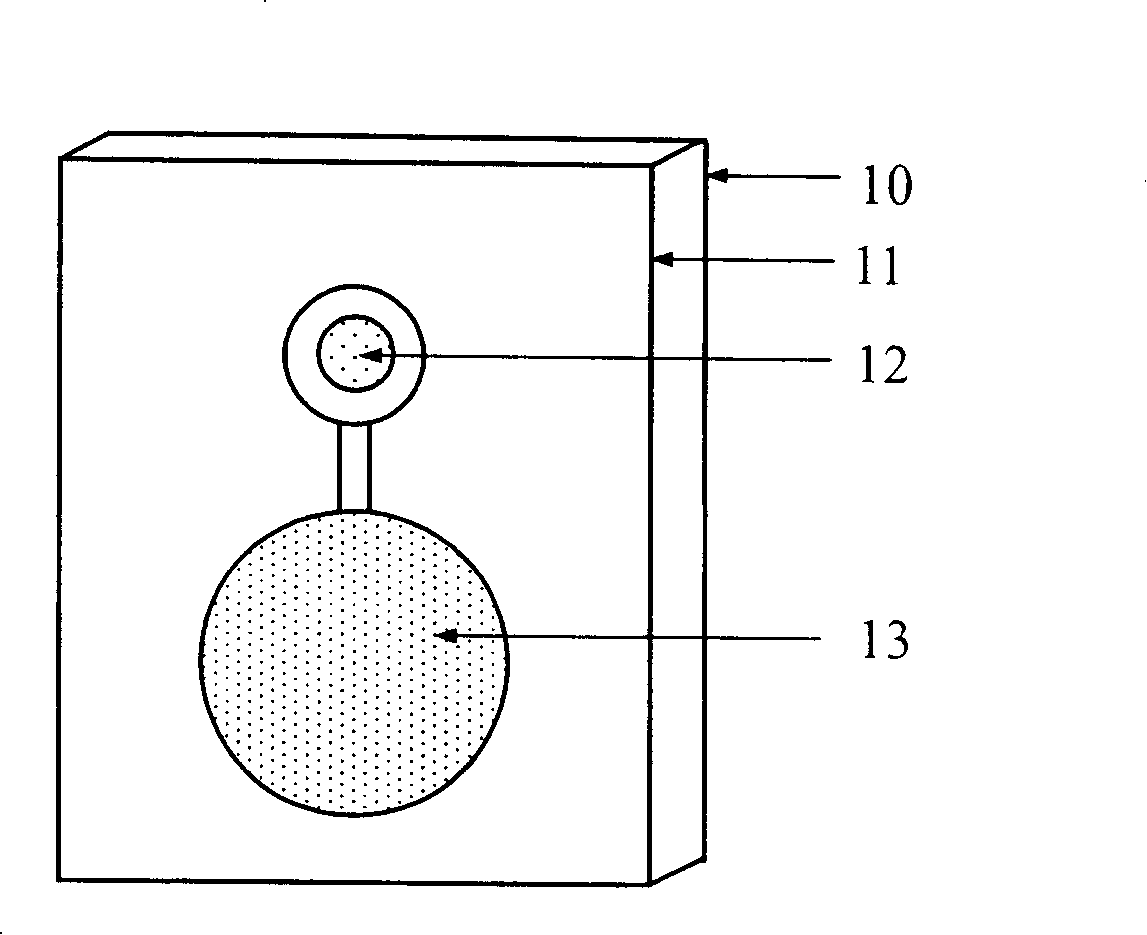
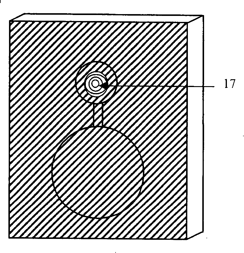
[0033] The vertical-cavity surface-emitting nanoscale semiconductor laser light source with surface plasmon modulation effect of the present invention is prepared on the basis of common vertical-cavity surface-emitting lasers. It is prepared on the basis of common vertical cavity surface emitting laser. The specific preparation process includes coating a layer of anti-reflection film on the surface of the light exit cavity of the ordinary vertical cavity surface emitting laser, making a ring and other periodic structures on the anti-reflection film medium within the range of the light exit hole, removing the insulating layer on the P surface electrode and then plating A layer of metal film, and then use the method of focused ion beam etching to prepare a small hole of sub-wavelength size on the light exit hole, confine the light in the low-loss micro-resonator cavity, make the light exit through the tiny opening, and make a ring around the small hole Equal periodic structure, ...


PUM


Abstract

The invention provides a method which manufactures a vertical-cavity surface-emitting nano-scale semiconductor laser source with surface plasma modulation effect. The method is prepared on the base of normal vertical cavity surface emitting laser. The detailed process comprises that an antireflection coating layer is grown on the output cavity surface of the normal vertical cavity surface emitting laser; a sub-wavelength periodic structure is prepared on the antireflection coating of the cavity surface in the range of an output optical hole by a method of focused ion beam etching; a layer of metal film is plated after an insulation layer on a P-surface electrode is removed; after that, a hole with sub-wavelength dimension and a sub-wavelength periodic structure are prepared on the metal film of the output optical cavity surface by the method of focused ion beam etching; the light is restricted in a low-loss micro-resonant cavity and emitted through a slight opening to generate a near field light with high efficiency and high directivity.

Description

technical field [0001] The invention relates to a vertical cavity surface emitting nanoscale semiconductor laser light source, in particular to a vertical cavity surface emitting nanoscale semiconductor laser light source with surface plasma modulation effect. [0002] The present invention also relates to the preparation method of the above-mentioned laser light source Background technique [0003] Current optical data storage systems, such as CD or DVD, are far-field storage systems, and their storage density is limited due to the limitation of diffraction limit. Utilizing the evanescent wave in the near-field of the light source can break through the limitation of the diffraction limit and greatly increase the storage density. Therefore, high-density optical data storage has become a large field of near-field optical applications. If a tiny light source that breaks through the diffraction resolution limit can be manufactured, it will be a great impetus to the application...

Claims


Application Information

Patent Timeline
Patent Type & Authority Applications(China)
IPC IPC(8): H01S5/183
Inventor 宋国峰高建霞郭宝山陈良惠
Owner INST OF SEMICONDUCTORS - CHINESE ACAD OF SCI
Why Eureka
Try Eureka