
On-chip test method for microwave power amplifier chip and its test system

A microwave power and amplifier technology, applied in the field of microwave power amplifier chip on-chip testing, can solve the problems of high price, influence, and unfavorable scientific research activities, so as to avoid packaging, reduce costs, and avoid time and economic losses. Effect

Inactive Publication Date: 2008-07-09
SHANGHAI INST OF MICROSYSTEM & INFORMATION TECH CHINESE ACAD OF SCI
View PDF0 Cites 33 Cited by
  • Summary
  • Abstract
  • Description
  • Claims
  • Application Information

AI Technical Summary

Problems solved by technology

The test system built in this way can achieve the goal, but the negative effect is that it is not only expensive, but also easily affected by the relevant instrument suppliers in practical applications, which is not conducive to the smooth development of scientific research activities

Method used


Image

  • On-chip test method for microwave power amplifier chip and its test system
  • On-chip test method for microwave power amplifier chip and its test system
  • On-chip test method for microwave power amplifier chip and its test system

Examples


Embodiment Construction

[0028] The substantive features and remarkable progress of the present invention will be further described below in conjunction with the accompanying drawings.

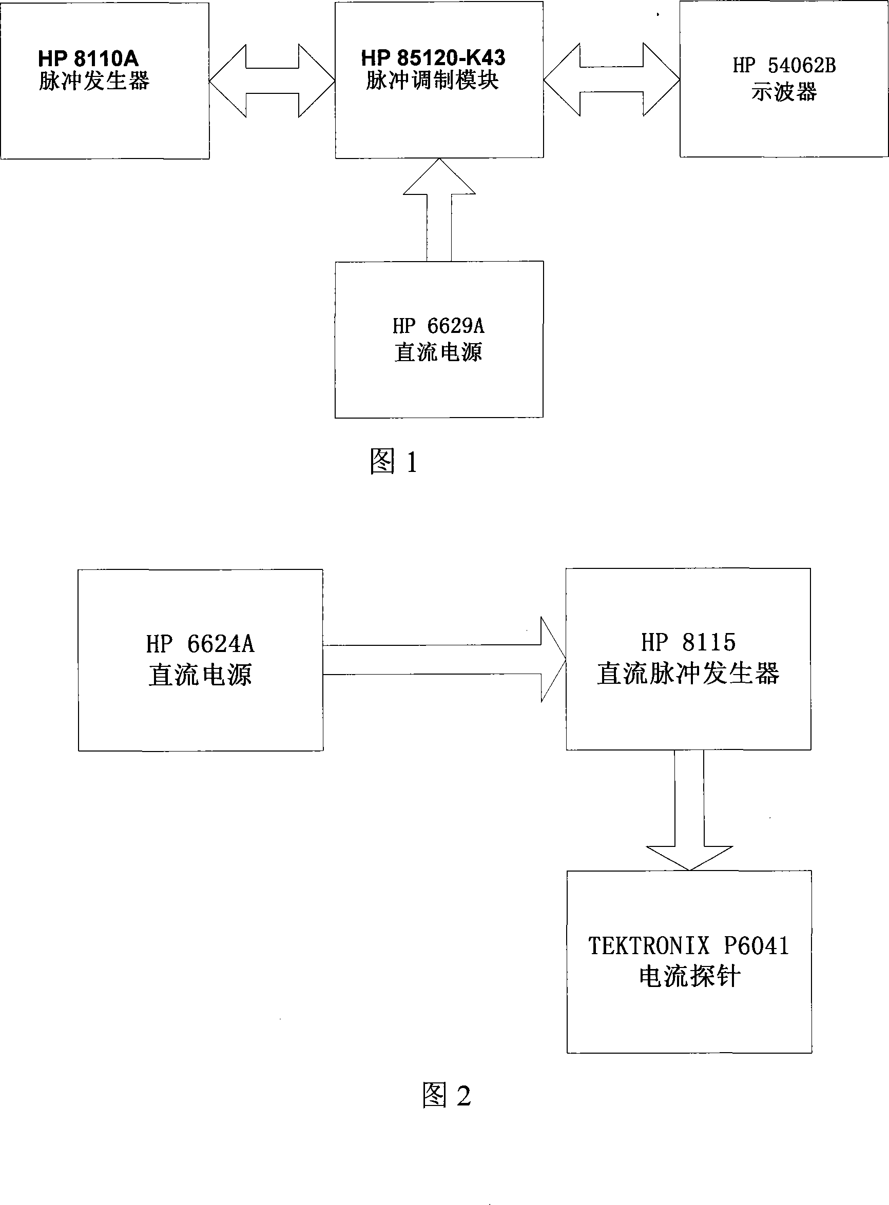
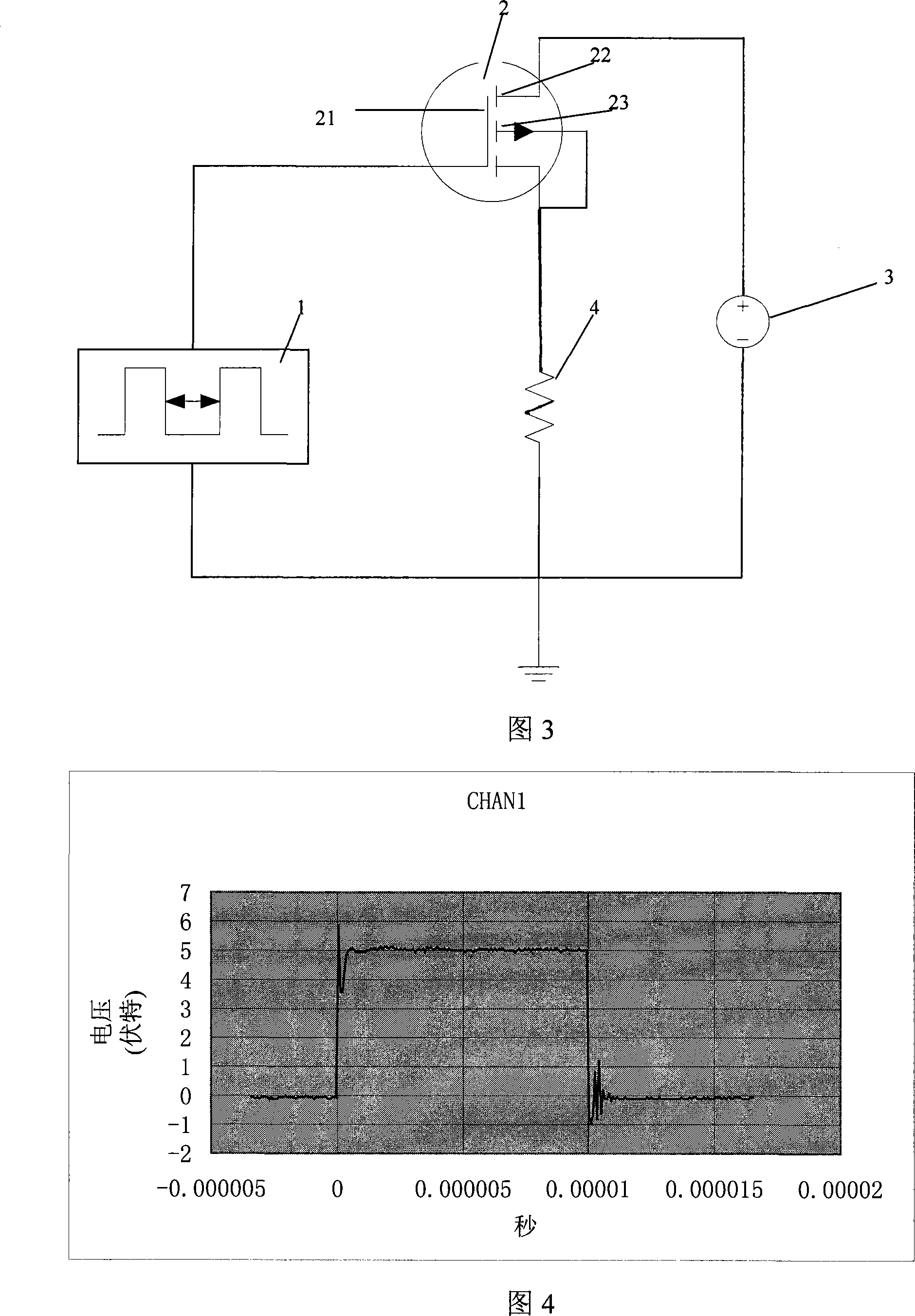
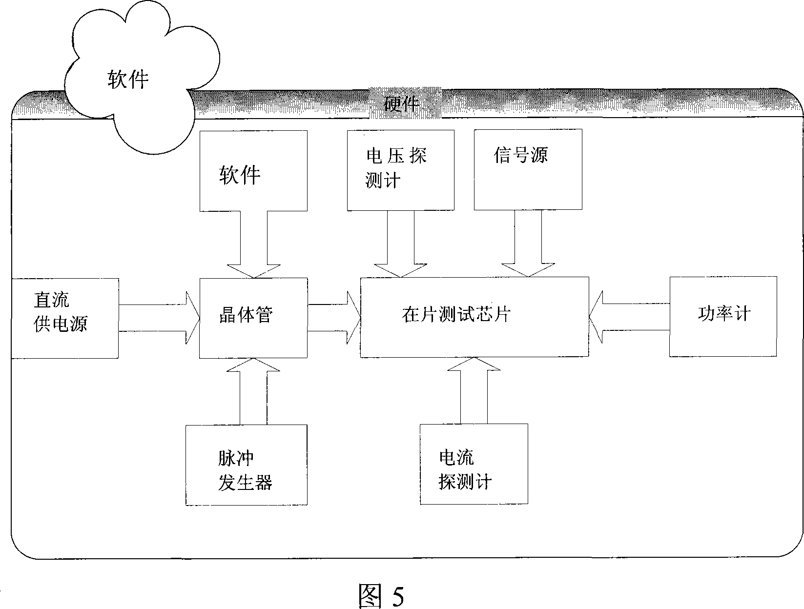
[0029] The pulse modulation and generating device designed by the present invention will be described in detail as follows with reference to examples and accompanying drawings. As shown in Figures 3 and 5, a test platform is built, 1 is a signal generator, 2 is a transistor, and 3 is a DC power supply required to meet the working point of the DUT. In a specific application, the DC power supply is connected to the drain 22 of the transistor, the pulse signal generator is connected to the gate 21 of the transistor, the DUT is connected to the source 23 of the transistor, and a voltage is applied to the connection line of the DUT 4 A current detector, applying power to make the DUT 4 work at a specified DC operating point.

[0030] Start the instrument according to the flow chart shown in Figure 6, first turn on the sig...


PUM


Abstract

The invention relates to a method for on-chip test of a microwave power amplifier chip and a test system thereof, which belong to the field of chip test technology of microwave communication. The invention is characterized in that a pulse-type bias voltage greatly reduces the influence of heat on the performance of a microwave power amplifier, thus authentically achieving on-chip test on probe test of a chip and obviating the installation of a package and an external heat dissipation system. A pulse modulation and pulse generation device modulates a pulse signal as the bias of the microwave power amplifier by use of the switch characteristics of a transistor. The DC pulse signal is connected with the gate of the transistor as the gate voltage to control the on / off of a transistor channel. When a positive voltage pulse signal is applied, the transistor channel is constructed so that a current source connected with the drain of the transistor can be applied on a source load through the channel; when a zero pulse signal is applied, the transistor channel is cutoff to prevent the current source from flowing to the source through the channel, so that no current passes through the load.

Description

technical field [0001] The invention relates to an on-chip testing method and system for microwave power amplifier chips. The method is suitable for microwave power amplifier chips in various frequency bands, and is widely used in power testing and gain testing of various microwave power amplifiers. The invention belongs to the technical field of chip testing in microwave communication. Background technique [0002] For GaAs FET (Gallium Arsenide Field Effect Transistor) devices, the channel temperature has a great influence on its radio frequency characteristics and DC characteristics, which is due to the fact that the GaAs substrate does not have a good heat sink capability; this Characterization is particularly prominent in probe station-based on-wafer testing of power chips. As the channel temperature rises, the characteristics of the chip show a tendency to deteriorate sharply. Therefore, a pulse bias measurement system based on isothermal environment is proposed. ...

Claims


Application Information

Patent Timeline
IPC IPC(8): G01R31/28
Inventor 张健孙晓玮李凌云顾建忠钱蓉
Owner SHANGHAI INST OF MICROSYSTEM & INFORMATION TECH CHINESE ACAD OF SCI
Learn More