A high voltage P-type MOS transistor and the corresponding manufacturing method
A semiconductor tube, oxide technology, applied in the direction of semiconductor/solid-state device manufacturing, semiconductor devices, electrical components, etc., can solve problems such as incompatibility, achieve good compatibility, reduce the longitudinal electric field of the channel, and reduce hot carrier injection effect of phenomenon
- Summary
- Abstract
- Description
- Claims
- Application Information
AI Technical Summary
Problems solved by technology
Method used
Image

Examples
Embodiment 1
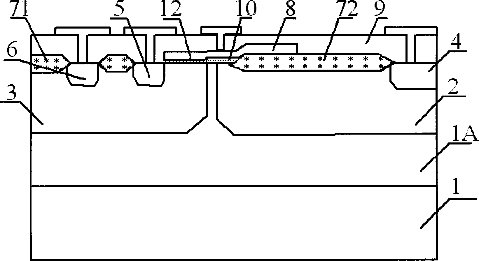
[0014] A high-voltage P-type metal oxide semiconductor tube, including a P-type substrate 1, a deep N-type well 1A is arranged on the P-type substrate 1, and an N-type well 3 and a P-type drift are arranged on the deep N-type well 1A Region 2, N-type contact hole 6, P-type source 5 and field oxide layer 71 are provided on N-type well 3, P-type drain 4 and field oxide layer 72 are provided on P-type drift region 2, and N-type well 3. A gate oxide layer is provided above the P-type drift region 2 and part of the deep N-type well 1A, and the gate oxide layer is located between the P-type source 5 and the field oxide layer 72 on the P-type drift region 2. On the gate oxide layer A polysilicon gate 8 is provided on it, and the polysilicon gate 8 extends to the field oxide layer 72 on the P-type drift region 2. On the field oxide layer 71, the N-type contact hole 6, the P-type source 5, the polysilicon gate 8, and the field oxide layer 72 And the P-type drain 4 is provided with an o...
Embodiment 2
[0016] A method for preparing a high-voltage P-type metal oxide semiconductor tube. First, select a P-type substrate, prepare a deep N-type well on the P-type substrate, prepare an N-type well and a P-type drift region on the deep N-type well, and then Preparation of field oxide layer, followed by growth and etching of thick gate oxide layer, after that, growth of thin gate oxide layer, followed by growth and etching of polysilicon gate, preparation of source and drain implantation regions and substrate contact implantation area, and finally the lead holes, the preparation and passivation of aluminum leads. The entire process can be realized on the basis of standard epitaxial low-voltage metal-oxide-semiconductor process lines.
PUM
 Abstract
Description
Claims
Application Information
 - R&D
- Intellectual Property
- Life Sciences
- Materials
- Tech Scout
- Unparalleled Data Quality
- Higher Quality Content
- 60% Fewer Hallucinations
Browse by: Latest US Patents, China's latest patents, Technical Efficacy Thesaurus, Application Domain, Technology Topic, Popular Technical Reports.
© 2025 PatSnap. All rights reserved.Legal|Privacy policy|Modern Slavery Act Transparency Statement|Sitemap|About US| Contact US: help@patsnap.com