
A structure of semiconductor luminous device with wide spectrum photo-emission function

A light-emitting device and wide-spectrum light technology, which is applied to semiconductor devices, electrical components, circuits, etc., can solve problems such as instability, drastic changes in emission spectrum, and reduced structural luminescence performance, to eliminate phase separation, reduce point defects, reduce The effect of the small piezoelectric effect

Inactive Publication Date: 2008-07-09
NANJING UNIV
View PDF0 Cites 12 Cited by
  • Summary
  • Abstract
  • Description
  • Claims
  • Application Information

AI Technical Summary

Problems solved by technology

The disadvantage is that the spectrum of the emitted light changes too drastically with different injection levels, showing a certain degree of instability
This method of selective growth has serious shortcomings. The main problem is that there are a large number of concentrated defects at the junction of the growth planes of different crystal planes. reduce

Method used


Image

  • A structure of semiconductor luminous device with wide spectrum photo-emission function
  • A structure of semiconductor luminous device with wide spectrum photo-emission function

Examples


Embodiment Construction

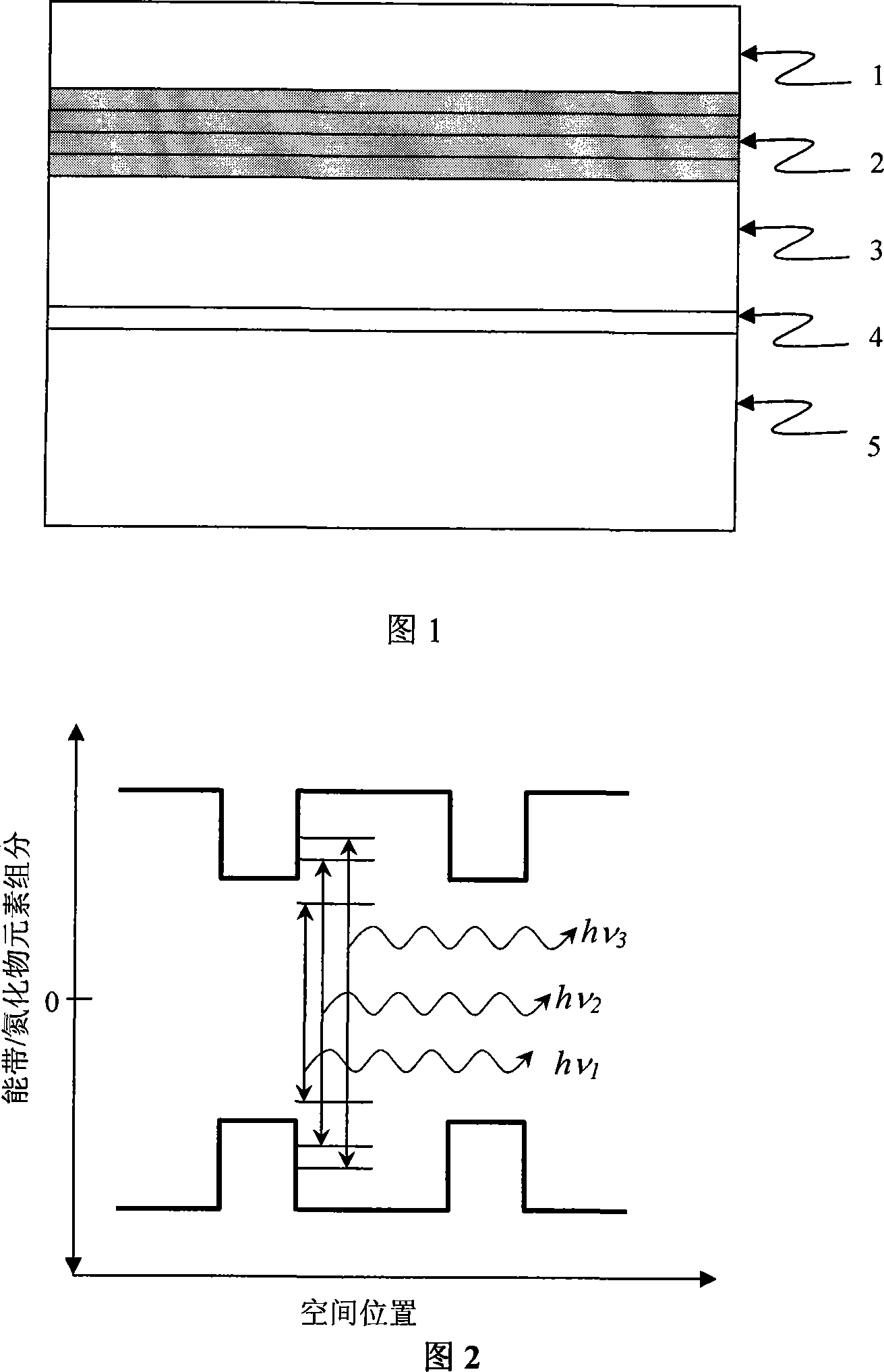
[0025] The examples illustrate the implementation of the invention, but the implementation of the invention is not limited to the implementation of the examples. Fig. 1 In the device structure of the present invention: 1 top layer nitride: such as p-GaN, 2 multilayer active region: such as InGsN quantum well, 3 bottom layer nitride: such as n-GaN, 4 transition layer: such as low temperature GaN, 5 lining Bottom material: such as sapphire.

[0026] The present invention utilizes the MOCVD (metal organic chemical vapor phase epitaxy) epitaxial growth system, adopts the method of synthesizing the multi-quantum well structure of nitride semiconductor with multi-energy level recombination function, and obtains the multi-energy level wide-spectrum light spectrum with nitride semiconductor as the basic material. emission. Specifically include the following steps:

[0027] 1. Surface cleaning and treatment of sapphire (0001) substrate. Clean the sapphire (0001) substrate with trich...


PUM


Abstract

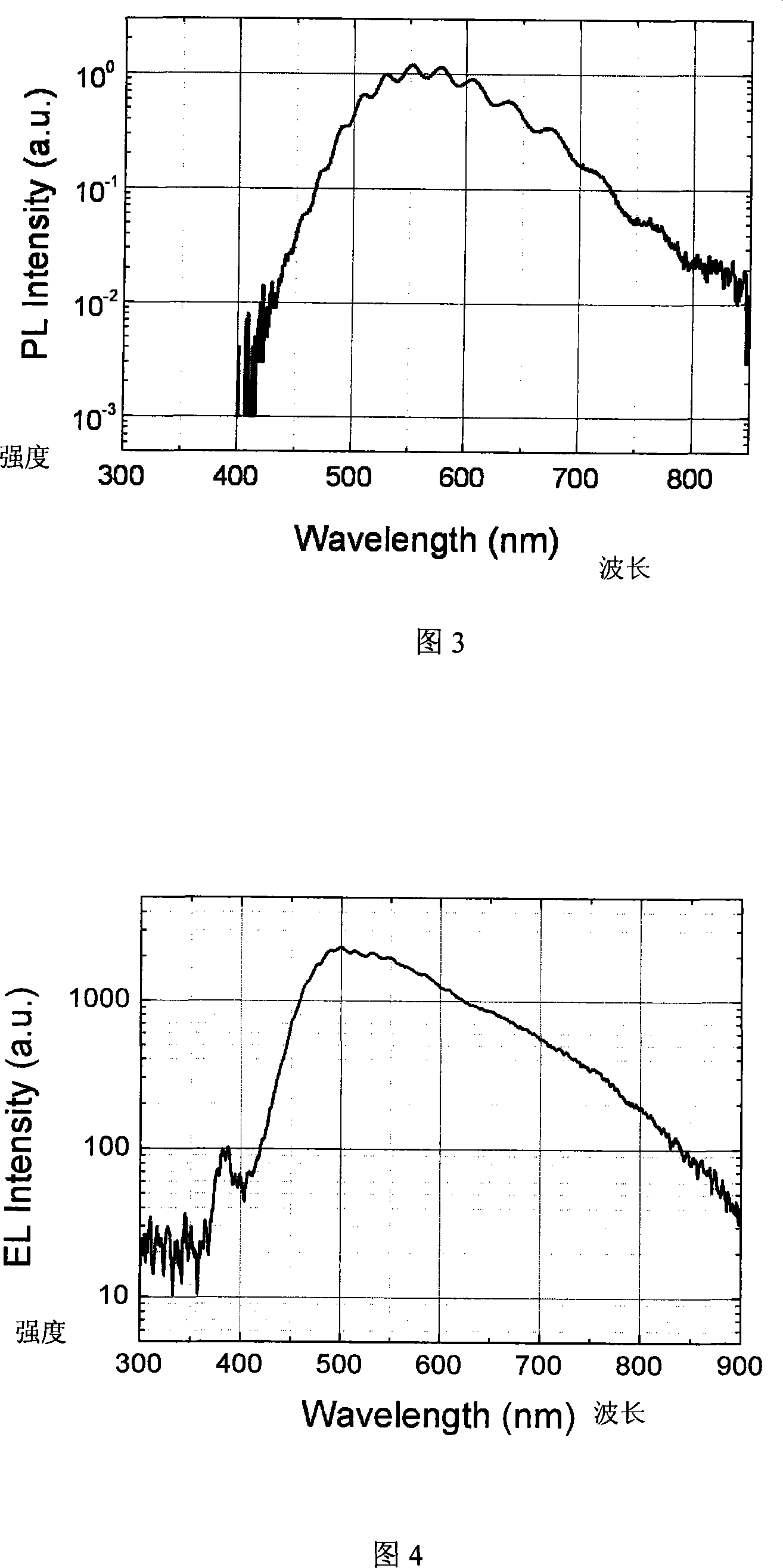
The invention relates to a semiconductor light-emitting device with wide spectrum light emission function and the preparation method, including a substrate material, a transition layer which directly grows on the substrate and a GaN or n-GaN which is arranged on the transition layer, a plurality of layers of quantum well active regions: a nitride quantum structure luminous layer with the wide spectrum light emission function is a quantum well structure, which is composed of an InxGa1-xN well layer and an InyGa1-yN barrier layer, wherein, 1 is more than x which is more than y which is not less than 0, the x and y in the quantum well structure is spacially even in the layers; the well / barrier double layers of the quantum well structure repeat 1 to 10 periods; a top layer nitride, GaN or p-GaN, the thickness of the top layer nitride is 0.02 to 2 microns; the invention further comprises multiple luminous centers which can emit light which contains the continuous spectrum with the nano-scope of 360 to 900. The nitride semiconductor material is obtained by the epitaxial growth of a metal-organic chemical vapor deposition (MOCVD) epitaxial growth system.

Description

1. Technical field [0001] The invention relates to a semiconductor light-emitting device and a preparation method, in particular to a method for realizing wide-spectrum multi-band light-emitting by using a novel semiconductor quantum structure. 2. Technical Background [0002] Semiconductor optoelectronic devices play an increasingly important role in scientific research and everyday life. The increasingly wide range of practical applications places more diverse requirements on optoelectronic devices. Semiconductor light-emitting devices have the advantages of small size, high efficiency and long life, and are widely used in the fields of indication, display and lighting. According to the intrinsic band structure of semiconductor materials, electron-hole radiative recombination usually occurs in a very limited energy range. At this time, semiconductor light-emitting devices usually have a narrow emission spectrum, that is, very good monochromaticity, which is a very good c...

Claims


Application Information

Patent Timeline
IPC IPC(8): H01L33/00H01L33/06
Inventor 陈鹏张荣郑有炓谢自力江若琏韩平胡立群施毅顾书林修向前朱顺明刘斌
Owner NANJING UNIV
Learn More