

Semiconductor component with dual whole metal silicide grids and manufacturing method thereof
A technology of metal silicide and metal silicide layer, which is applied in semiconductor/solid-state device manufacturing, semiconductor devices, electrical components, etc., can solve the problems of complicated process and unable to reduce manufacturing cost, and achieve the effect of simplifying process steps and saving costs
- Summary
- Abstract
- Description
- Claims
- Application Information
AI Technical Summary
Problems solved by technology
Method used
Image

Examples
no. 1 example
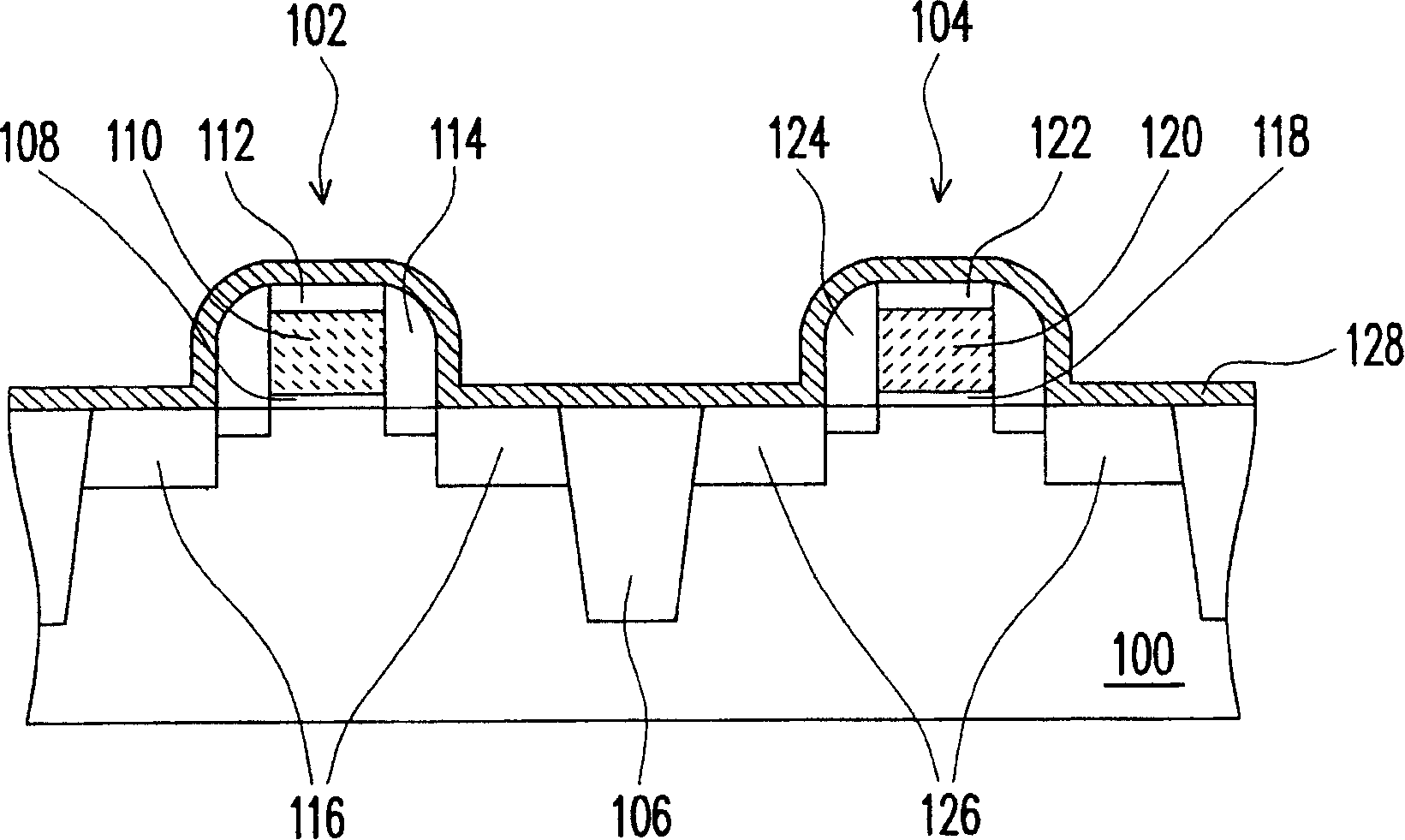
[0108] Figure 1A to Figure 1D It is a process cross-sectional view illustrating a manufacturing method of a semiconductor device with double full metal silicide gates according to the first embodiment of the present invention.
[0109] Please refer to Figure 1A , first provide a substrate 100 . The substrate 100 includes a silicon substrate, such as an N-type silicon substrate or a P-type silicon substrate. Certainly, the substrate 100 may also be a substrate with silicon on an insulating layer or the like.
[0110] A transistor 102 and a transistor 104 have been formed on the substrate 100 . The transistor 102 and the transistor 104 are isolated by, for example, an element isolation structure 106 . The device isolation structure 106 is, for example, a shallow trench isolation structure or a field oxide layer.
[0111] The transistor 102 is composed of, for example, a gate dielectric layer 108 , a gate 110 , a cap layer 112 , a spacer 114 and a source / drain 116 .
[011...
no. 2 example
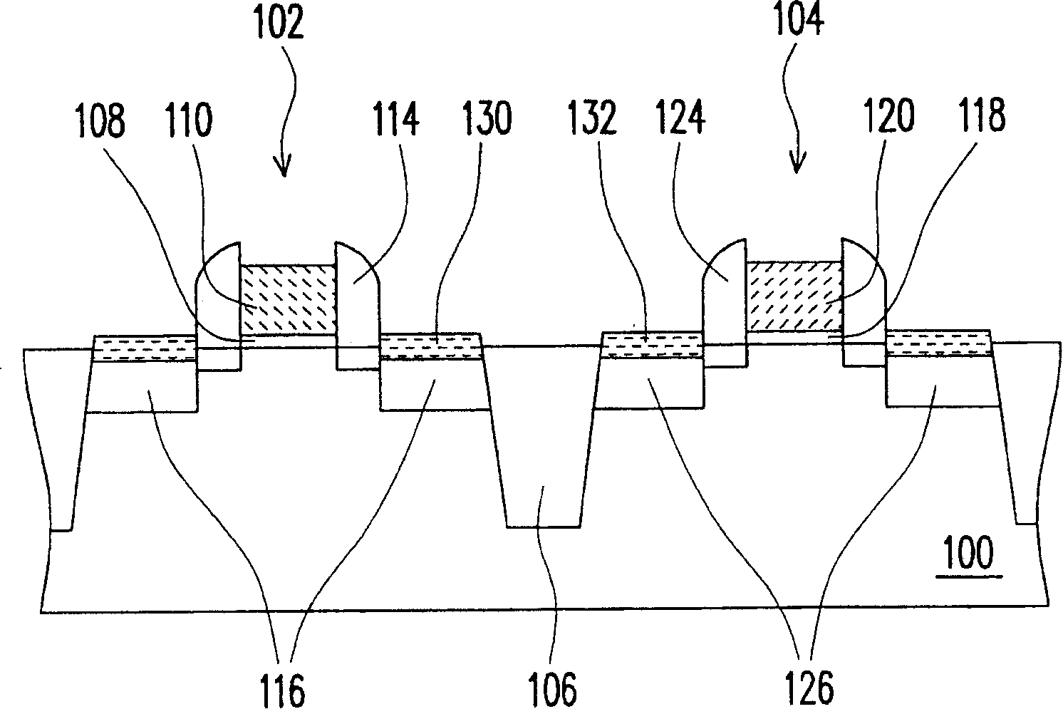
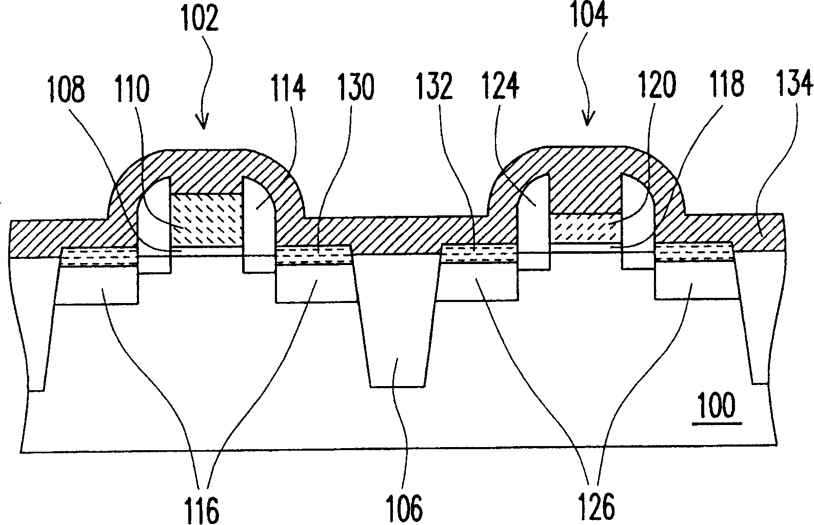
[0143] Figure 2A to Figure 2D It is a process cross-sectional view illustrating a method for manufacturing a semiconductor device with double full metal silicide gates according to the second embodiment of the present invention. The second embodiment is a modified example of the first embodiment. In the second embodiment, components that are the same as those in the first embodiment are given the same reference numerals, and description thereof will be omitted.
[0144] Please refer to Figure 2A , first provide a substrate 100 . The substrate 100 includes a silicon substrate. A transistor 102 and a transistor 104 have been formed on the substrate 100 . The transistor 102 and the transistor 104 are isolated by, for example, an element isolation structure 106 . The transistor 102 is composed of, for example, a gate dielectric layer 108 , a gate 110 , a cap layer 112 , a spacer 114 and a source / drain 116 . The transistor 104 is composed of, for example, a gate dielectric l...
no. 3 example
[0156] Figure 3A to Figure 3D It is a process cross-sectional view illustrating a method for manufacturing a semiconductor device with double all-metal silicide gates according to a third embodiment of the present invention.
[0157] Please refer to Figure 3A , first provide the substrate 200 . The substrate 200 includes a silicon substrate, such as an N-type silicon substrate or a P-type silicon substrate. Of course, the substrate 200 may also be a substrate with silicon on an insulating layer or the like.
[0158] A transistor 202 and a transistor 204 have been formed on the substrate 200 . The transistor 202 and the transistor 204 are isolated by, for example, an element isolation structure 206 . The device isolation structure 206 is, for example, a shallow trench isolation structure or a field oxide layer.
[0159]The transistor 202 is composed of, for example, a gate dielectric layer 208 , a gate 210 , a spacer 214 and a source / drain 216 . The transistor 204 is co...
PUM
 Abstract
Description
Claims
Application Information