Thin film transistor array base plate and its making method

A technology of thin film transistors and array substrates, which is applied in the field of self-repairing thin film transistor array substrates and its manufacturing, can solve the problems of rising manufacturing costs, increasing signal delays, increasing wiring film thickness, etc., to reduce production costs, reduce signal delays, The effect of increasing the number of masks

Inactive Publication Date: 2008-08-06
NANJING CEC PANDA LCD TECH
View PDF1 Cites 10 Cited by
  • Summary
  • Abstract
  • Description
  • Claims
  • Application Information

AI Technical Summary

Problems solved by technology

[0003] However, as the display area of ​​the display device increases, the scanning wiring connected to the TFT becomes longer and longer, causing an increase in wiring resistance, resulting in an increase in signal delay, which poses a problem for in-plane uniform display
In order to reduce the signal delay caused by the increase in resistance, Chinese published patents 200610132270.3 and 200610099012 propose the use of copper wiring with lower resistance, but the copper process is less compatible with the existing process and may cause other problems
The traditional method is to increase the width of the wiring, which reduces the aperture ratio and leads to an increase in cost; in addition, the film thickness of the wiring is increased, and the increase in the film thickness of the wiring brings about an increase in cost and a change in the step coverage. Poor, resulting in a decline in product yield
[0004] In addition, during the manufacturing process of the thin film transistor array substrate, scanning disconnection defects may occur
When the scanning wiring defect occurs on the thin film transistor array substrate, if the disconnection is not repaired, the manufacturing yield of the thin film transistor array substrate will be greatly reduced, resulting in a significant increase in manufacturing costs. Therefore, it is necessary to disconnect the scanning wiring. For repair, laser repair method is commonly used at present, which leads to complicated manufacturing process and increased manufacturing cost

Method used


Image

  • Thin film transistor array base plate and its making method
  • Thin film transistor array base plate and its making method
  • Thin film transistor array base plate and its making method

Examples


Embodiment Construction

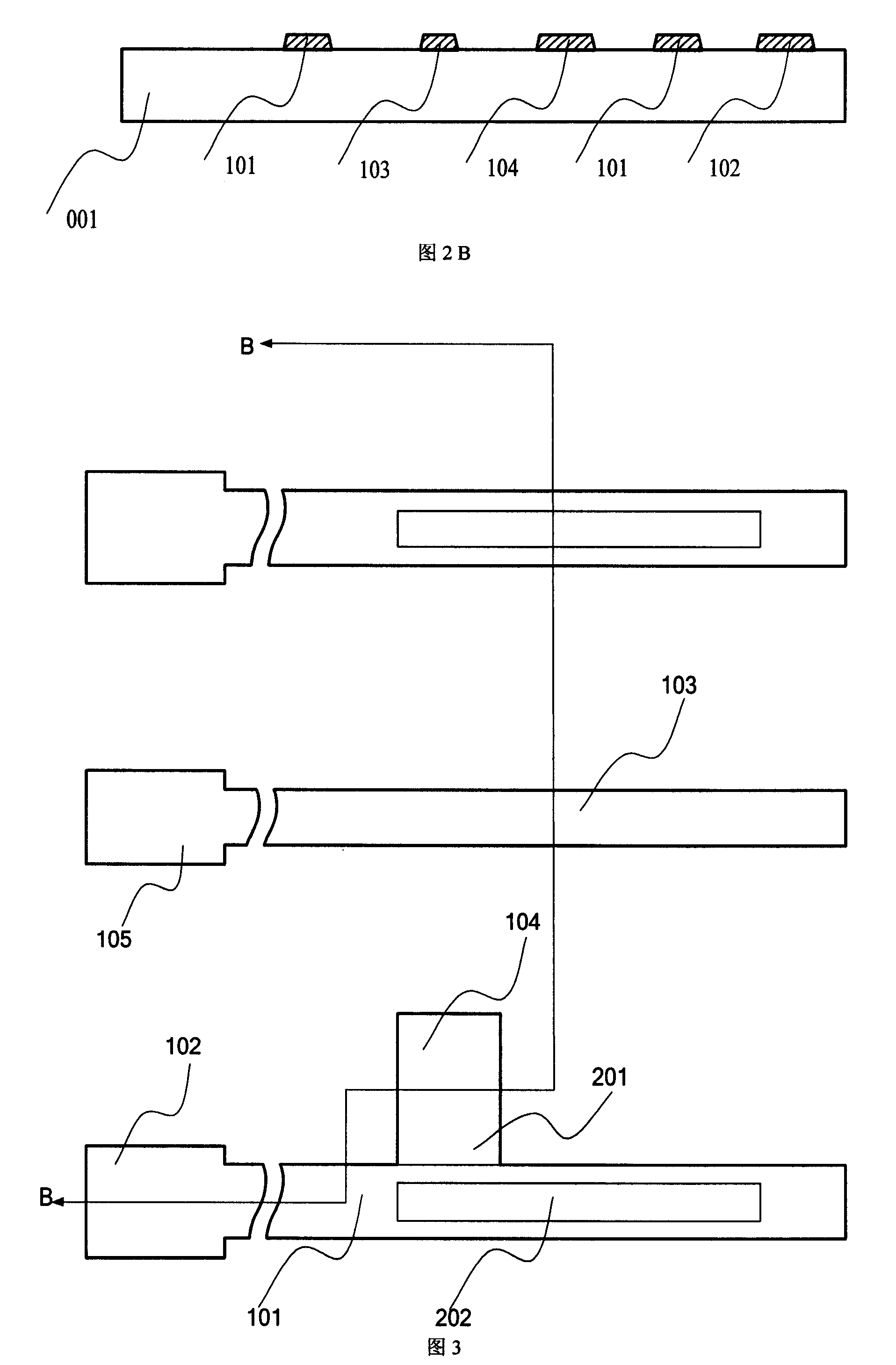
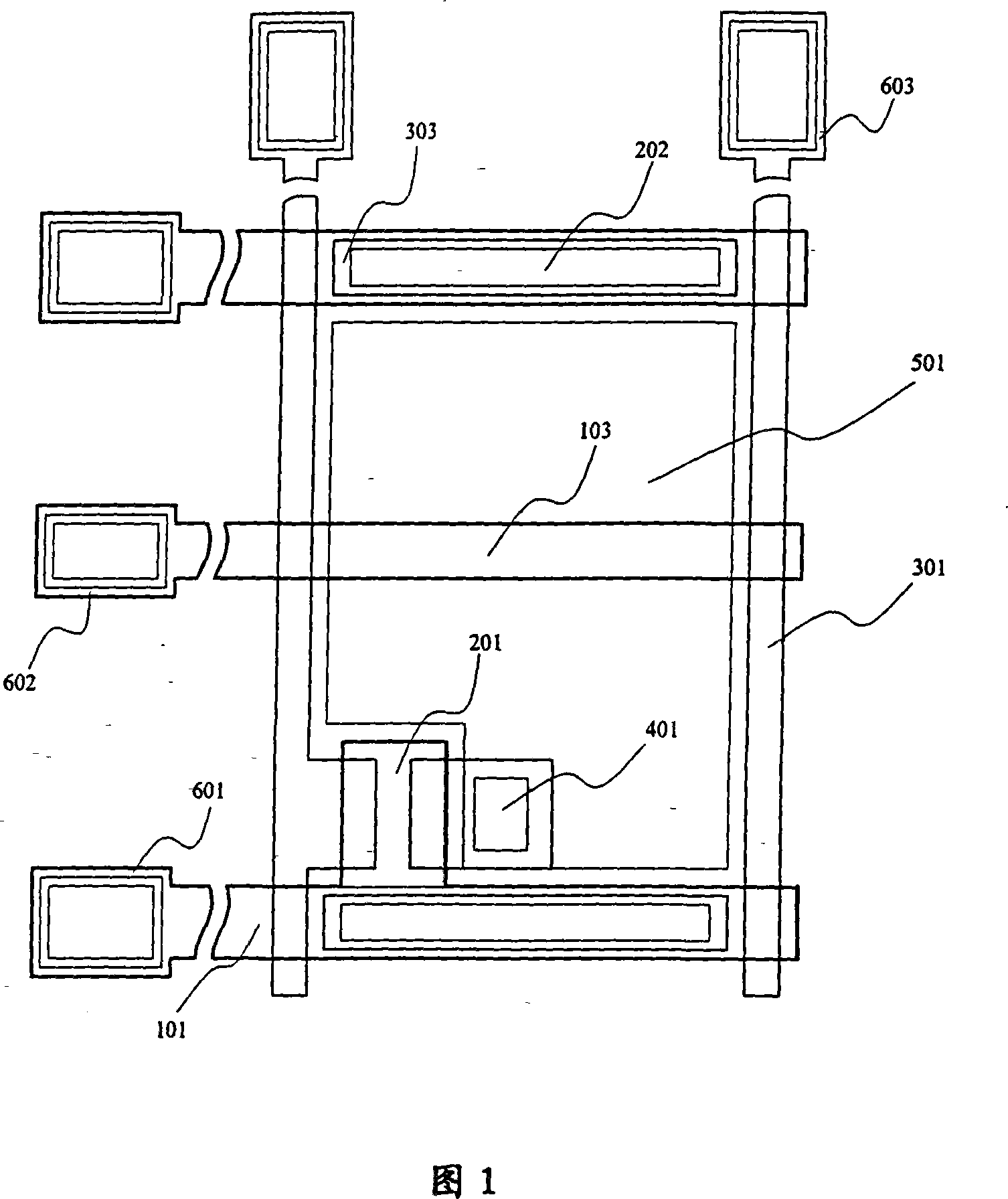
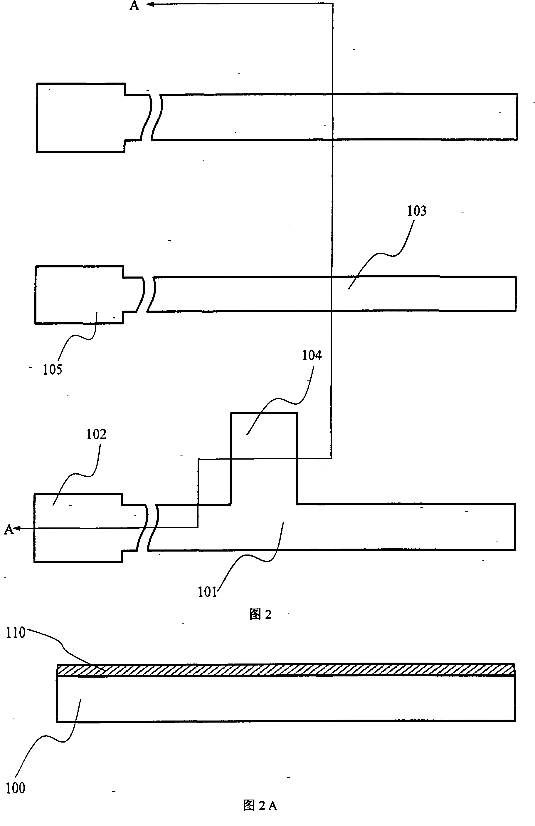
[0035] 1 to 6, the thin film transistor array substrate of the present invention has a scanning wiring conductive layer 110, an insulating layer 201, a data conductive layer 310, a passivation insulating layer 410 and a transparent conductive layer 510 sequentially formed on an insulating substrate 100, so that The insulating substrate 100 is a glass substrate or a plastic substrate; the scanning wiring 101 and the common electrode line 103 are formed on the scanning wiring conductive layer 110, and the gate insulating film 210, the semiconductor layer 220 and the ohmic In the contact layer 221 , the gate insulating film 210 does not cover or partly covers the scan wiring 101 , and the exposed scan wiring 202 is in direct electrical contact with the data wiring 303 on the above data conductive layer 310 .

[0036] The specific manufacturing method is described in conjunction with FIG. 2 to FIG. 6 .

[0037] First, referring to FIGS. 2, 2A and 2B, a scanning wiring conductive l...


PUM


Abstract

The invention discloses a thin film transistor array substrate and a method for manufacturing the same. The thin film transistor array substrate is provided with a scanning wiring conductive layer, an insulation layer, a data conductive layer, a passivation insulation layer and a transparent conducive layer in sequence. The scanning wiring conductive layer is provided with a scanning wiring and a common electrode line; the insulation layer comprises a gate insulating film; the scanning wiring is at least partially exposed and is in direct electric contact with the data conductive layer above; the array substrate of the structure can reduce signal delay of the scanning wiring and can also realize self-repair when the scanning wire breaks without a special repairing line being arranged.

Description

technical field [0001] The invention relates to an array substrate and a manufacturing method thereof, in particular to a self-repairable thin film transistor array substrate capable of reducing wiring signal delay and a manufacturing method thereof. Background technique [0002] A liquid crystal display (LCD) is a flat panel display widely used at present, and has the characteristics of low power consumption, thin appearance, light weight, and low driving voltage. Thin-film transistor liquid crystal display (TFT-LCD) is the most important type of liquid crystal display, which has the advantages of small size, light weight, and no radiation. A thin film transistor liquid crystal display generally includes a liquid crystal display panel and a backlight module. Wherein, the liquid crystal display panel includes a thin film transistor array substrate, a color filter substrate and a liquid crystal layer arranged between the two substrates. The display area of ​​the liquid crys...

Claims


Application Information

Patent Timeline
Patent Type & Authority Applications(China)
IPC IPC(8): H01L23/522H01L27/12H01L21/768H01L21/84G02F1/1362
Inventor 李喜峰李俊峰
Owner NANJING CEC PANDA LCD TECH
Why Eureka
Try Eureka