
Quanta point resonance tunnel penetration diode for faint light detection and its detection method

A resonant tunneling and quantum dot technology, applied in the field of visible light and short-wave infrared detectors, can solve the problems of difficulty in increasing the magnification of photogenerated carriers, too small tunneling current, hindering applications, etc., and achieve ultra-high photon detection capability. , the device structure is simple, the effect of ultra-high sensitivity

Active Publication Date: 2008-08-06
SHANGHAI INST OF TECHNICAL PHYSICS - CHINESE ACAD OF SCI
View PDF0 Cites 10 Cited by
  • Summary
  • Abstract
  • Description
  • Claims
  • Application Information

AI Technical Summary

Problems solved by technology

[0003] The disadvantages of this device are: (1) The operating temperature of the device is required to be at an ultra-low temperature of 5K, which makes the practical application of the device encounter great difficulties
(2) The amplification of photogenerated carriers in the photodetection process of the device is completed by the AlGaAs / GaAs / AlGaAs double barrier resonance tunneling effect, and the quantum dots only play a role in affecting the potential of the quantum well, and do not directly participate in the resonance tunneling process. In this way, the photogenerated carrier amplification factor of the device is difficult to continue to increase, which hinders its application at higher temperatures.
(3) The barrier layer is too thick, and the tunneling current is too small (peak current is less than 1nA), which is not conducive to the high-speed detection of photons

Method used


Image

  • Quanta point resonance tunnel penetration diode for faint light detection and its detection method
  • Quanta point resonance tunnel penetration diode for faint light detection and its detection method

Examples


Embodiment Construction

[0022] Below in conjunction with accompanying drawing and embodiment the specific embodiment of the present invention is described in further detail:

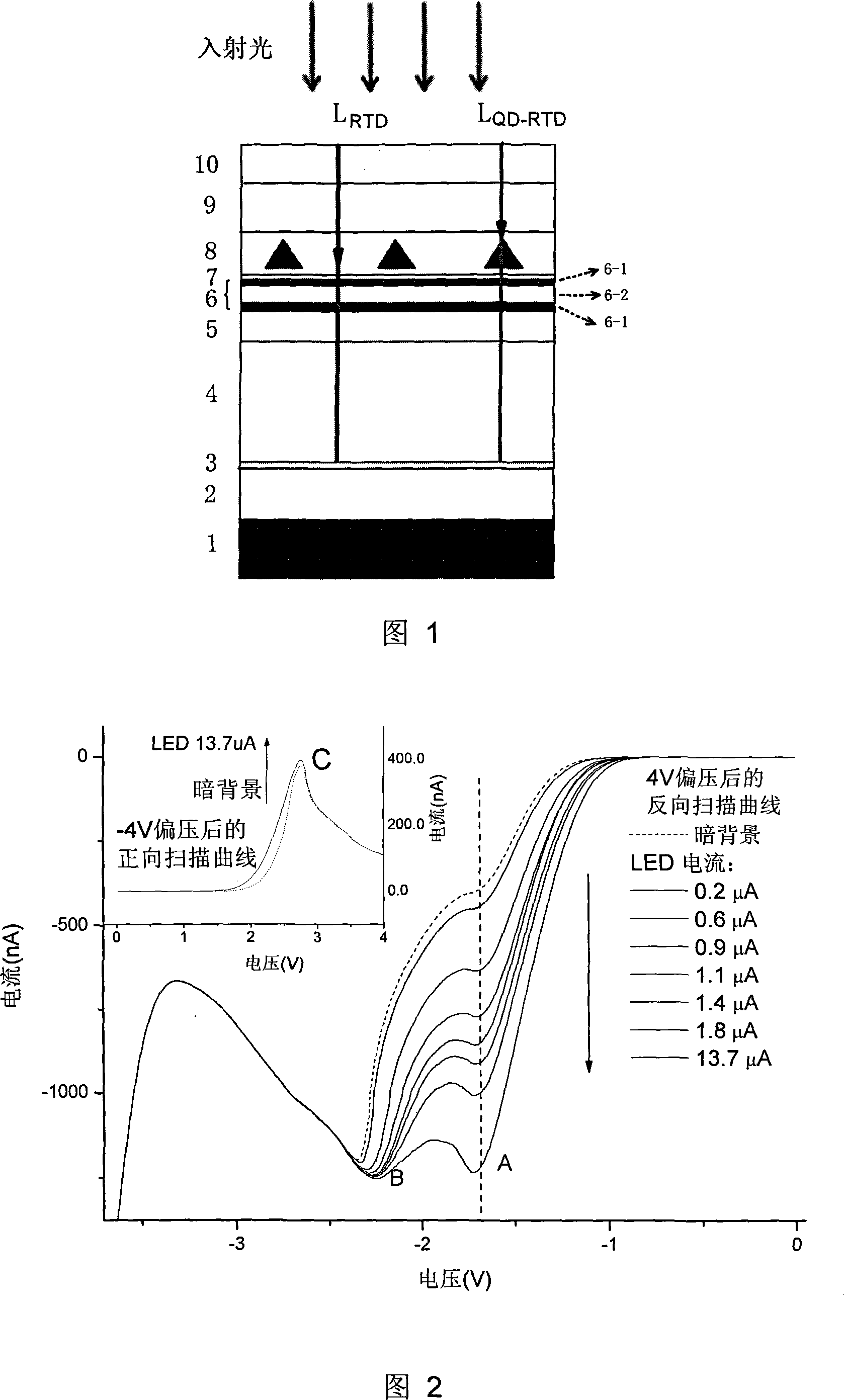
[0023] As shown in Figure 1, a 200nm GaAs buffer layer 2, a 10nm AlAs corrosion barrier layer 3, and a 380nm gradient n are sequentially grown on a semi-insulating GaAs substrate 1 by molecular beam epitaxy or metal organic vapor phase epitaxy. + GaAs (with a doping concentration of 1×10 18 -1×10 16 cm -3 ) lower electrode 4, 20nm GaAs spacer layer 5, 3nm AlAs barrier 6-1, 8nm GaAs potential well 6-2, 3nm AlAs barrier 6-1, 2nm GaAs spacer 7, the density is about 10 10 cm -2 InAs quantum dot layer 8, 150nm GaAs light absorption layer 9, 50nm n + GaAs (with a doping concentration of 2×10 18 cm -3 ) upper electrode 10. If the infrared band is to be detected, the GaAs absorption layer is changed to an InGaAs layer, and the photoresponse band can be modulated to short-wave infrared. AFM shows that the actual density of quant...


PUM


Abstract

The present invention discloses a quantum dot resonant tunneling diode for weak light detection and a detection method thereof, wherein, the quantum dot resonant tunneling diode comprises GaAs responsive to visible light or an InGaAs photon absorption region responsive to infrared, self-assembling quantum dots, a thin AlAs double barrier layer, and a GaAs potential well layer. The combination formed by the self-assembling quantum dots, the thin AlAs double barrier layer and the GaAs potential well layer allows the quantum dots to directly participate in the resonant tunneling process, the amplifying capacity of the resonant tunneling process upon photo-generated carriers is greatly improved. The detection method is as follows: filling carriers to the quantum dots to form a metastable state before incident light detection, and further improving the photoresponse capacity of devices. The diode and the detection method have the advantages that: the structure of the device is simple, the size and the density of the quantum dots are within a general growth range, and the manufacture is easy; the device obtains the photon detection with ultra high sensitivity at liquid nitrogen temperature.

Description

technical field [0001] The invention relates to a visible light and short-wave infrared detector, in particular to a quantum dot resonant tunneling diode used to detect visible light and short-wave infrared quantum dots directly participating in resonant tunneling and a detection method thereof. Background technique [0002] The double-barrier resonant tunneling diode (RTD) structure realized by semiconductor heterostructure can be traced back to 1974, and the resonant tunneling effect was observed in the AlGaAs barrier GaAs potential well structure. Resonant tunneling devices are mainly used in the electrical field, and have the advantages of high frequency, high speed, bistable, and self-locking. J.C. Blakesley et al first applied resonant tunneling to the field of high-sensitivity photon detection in 2005 (see Phys. Rev. Lett. 94, 067401 (2005)). They adopt a double barrier structure: Al x Ga 1-x As (x=0.33) potential barrier, its thickness is 10nm, GaAs potential well...

Claims


Application Information

Patent Timeline
IPC IPC(8): H01L31/11G01J1/42
Inventor 陆卫王旺平侯颖李天信陈平平张波甄红楼李宁陈效双
Owner SHANGHAI INST OF TECHNICAL PHYSICS - CHINESE ACAD OF SCI
Learn More