Organic electroluminescent element, display device, and lighting device
一种电致发光元件、致发光的技术,应用在电气元件、电固体器件、电路等方向,能够解决不能得到充分的效率等问题,达到良好发光亮度、黑点少、稳定性高的效果
- Summary
- Abstract
- Description
- Claims
- Application Information
AI Technical Summary
Problems solved by technology
Method used
Image
Examples
Embodiment 1
[0237] (Production of organic EL element 1-1)
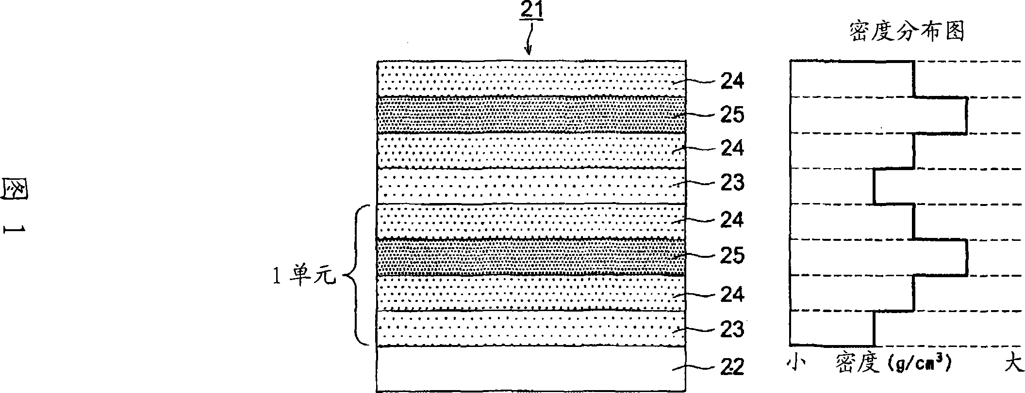
[0238] As a base material, on a polyethylene naphthalate film (made by Teijin DuPont, hereinafter abbreviated as PEN) with a thickness of 100 μm, under the following atmospheric pressure plasma discharge treatment apparatus and discharge conditions , making a substrate 1 having a gas barrier layer according to the cross-sectional view shown in FIG. 1 .
[0239] (Atmospheric pressure plasma discharge treatment device)
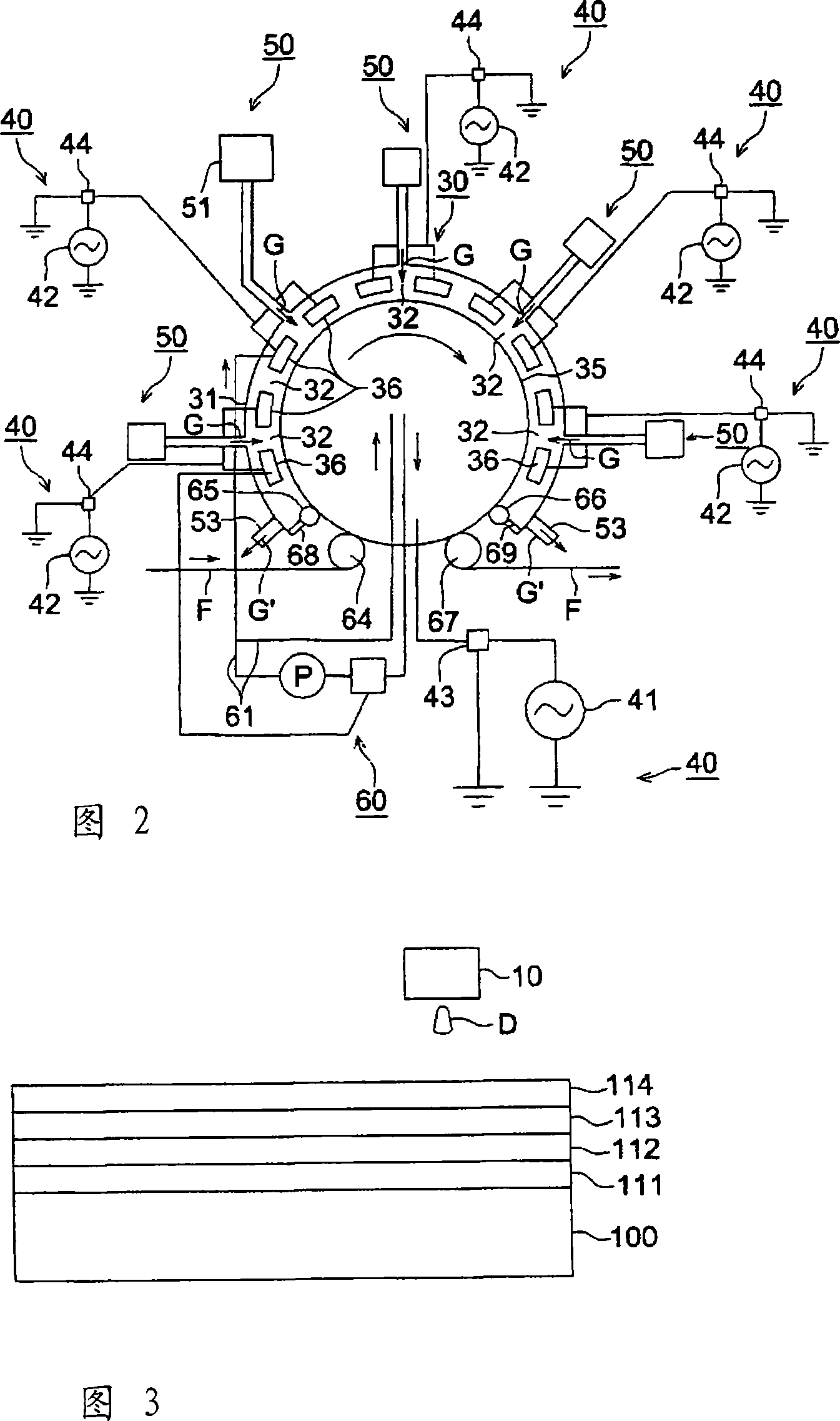
[0240] Using the atmospheric pressure plasma discharge treatment apparatus of FIG. 2 , a roll electrode covered with a dielectric and a plurality of square cylindrical electrode groups were produced as follows.
[0241] As the roll electrode of the first electrode, the titanium alloy T64 jacketed roll metal base material with a cooling water cooling device was coated with a high-density and high-adhesive aluminum sprayed film by the atmospheric plasma method to make the roll diameter 1000mmφ. On the other hand, f...
Embodiment 2
[0319] (Production of organic EL element 2-1)
[0320]Using a commercially available inkjet nozzle 10 in the same manner as in Example 1, the fluid containing the exemplified compound A36 and THF was ejected onto an ITO substrate 100, and a film with a film thickness of 50 nm was formed at 100° C. for 60 minutes. hole transport layer.
[0321] Next, a fluid containing the exemplified compound A31 as the main body, the phosphorescent compound Ir-12 (mass ratio 100:4) and THF was sprayed onto the hole transport layer, and a film was formed at 100° C. for 60 minutes. 50nm thick luminescent layer.
[0322] Next, a fluid containing the exemplified compound A35 and THF was sprayed onto the light-emitting layer, and an electron transport layer with a film thickness of 50 nm was formed at 100° C. for 60 minutes. Then, aluminum 113 (cathode) was vapor-deposited to a thickness of 200 nm on the electron transport layer.
[0323] In addition, the content rate of the organic solvent of ...
Embodiment 3
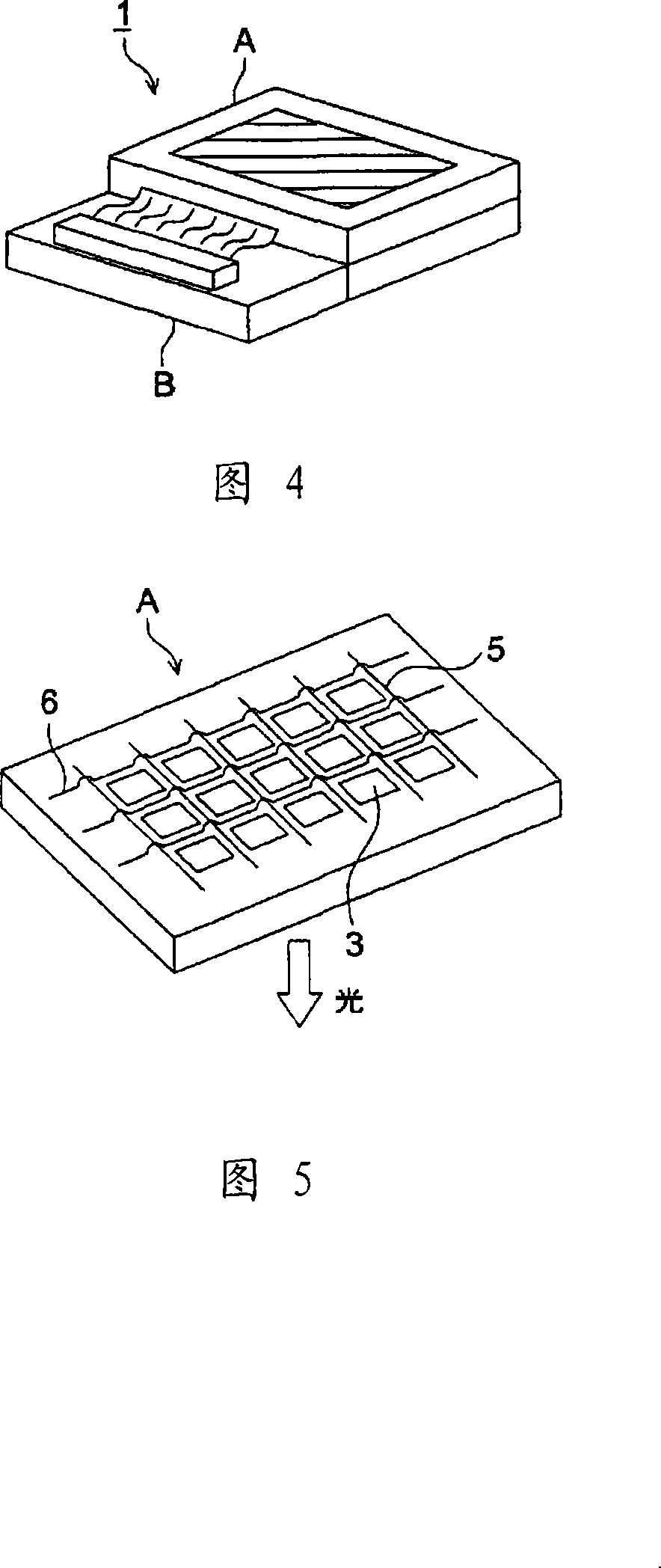
[0334] The organic EL element 2-4 of the present invention produced in Example 2, the phosphorescent compound of the organic EL element 2-4 of the present invention produced in Example 2 was changed to Ir-1, and the green light-emitting organic EL produced in the same way The red light-emitting organic EL element produced in the same way as the organic EL element 2-4 of the present invention except that the phosphorescent compound is changed to Ir-9 is arranged side by side on the same substrate, and the active matrix method full-color EL element shown in FIG. 4 is fabricated. display device. Fig. 5 shows only a schematic view of the display unit A of the fabricated full-color display device. That is, on the same substrate, there are wiring parts including a plurality of scanning lines 5 and data lines 6, and a plurality of pixels 3 arranged in parallel (pixels in a red area, pixels in a green area, and pixels in a blue area). Pixels, etc.), the scanning line 5 and a pluralit...
PUM
| Property | Measurement | Unit |
|---|---|---|
| density | aaaaa | aaaaa |
| density | aaaaa | aaaaa |
| density | aaaaa | aaaaa |
Abstract
Description
Claims
Application Information


