Oxygen silicon base doped nitride film yellow green wave band LED and its preparing method

A technology of light-emitting diodes and nitrides, which is applied in the direction of electrical components, circuits, semiconductor devices, etc., can solve the problems of weak light emission and high working current density, achieve low turn-on voltage, increase the density of light-emitting centers, and improve the effect of light-emitting characteristics

Inactive Publication Date: 2008-12-24
NANJING UNIV
View PDF4 Cites 0 Cited by
  • Summary
  • Abstract
  • Description
  • Claims
  • Application Information

AI Technical Summary

Problems solved by technology

[0005] Usually PECVD technology is used at conventional temperature (300°C) to SiH 4 and NO 2 Oxygen-containing a-SiN grown as a gas source x The thin film can realize photoluminescence at room temperature, but the light-emitting device using it as the active layer cannot realize electroluminescence at room temperature. It can only be realized after thermal annealing at 950°C, and the luminescence is weak and the working current density is high. See [5] K. J. Price, et al. J. Appl. Phys. 86 2638 (1999)

Method used


Image

  • Oxygen silicon base doped nitride film yellow green wave band LED and its preparing method
  • Oxygen silicon base doped nitride film yellow green wave band LED and its preparing method
  • Oxygen silicon base doped nitride film yellow green wave band LED and its preparing method

Examples


Embodiment Construction

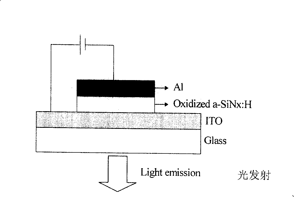
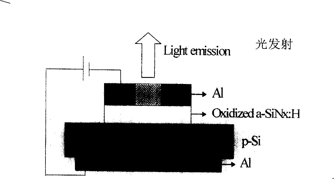
[0034] 1. Preparation of active layer of new silicon-based light-emitting devices

[0035] (1) Growth of amorphous silicon nitride (a-SiN) at room temperature x )film

[0036] Using plasma enhanced chemical vapor deposition (PECVD) technology, using silane (SiH 4 ) and ammonia (NH 3 ) as a reactant gas source, depositing a-SiNx film on a P-type single crystal silicon wafer with a resistivity of 4-20Ωcm and an ITO glass substrate. Concrete process conditions during preparation are as follows:

[0037] Power source frequency: 13.56MHz

[0038] Power density: 0.6W / cm 2

[0039] Reaction chamber pressure: 80Pa

[0040] Substrate temperature: 25°C

[0041] Depositing a-SiN x thin film, made of SiH 4 +NH 3 Formed by glow decomposition reaction, where SiH 4 The flow rate is 8sccm (standard cubic centimeters per minute), NH 3 The flow rate is 32sccm; the deposition time is 130s, and the film thickness is 80nm.

[0042] (2) Plasma oxidation of amorphous silicon nitride (a...


PUM

PropertyMeasurementUnit
thicknessaaaaaaaaaa
thicknessaaaaaaaaaa

Abstract

The related O-doped silicon-base nitride thin film yellow-green wave range LED comprises: a 40-100nm a-SiNx thin film deposited on 4-20Omegacm P-type monocrystal silicon wafer or ITO glass substrate, a thin film metal electrode coated on the a-SiNx film, a electrode on back of P-type wafer, a electrode formed by ITO itself for light emergence, and a 1ª–m Al thin film as cathode evaporation coated on the active layer. Wherein, the round Al electrode is 3mm in diameter.

Description

1. Technical field: [0001] The invention relates to a photoluminescent device and a preparation method. In particular, a novel oxygen-doped silicon nitride thin-film light-emitting diode is proposed from two aspects of light-emitting mechanism and preparation and implementation process. The active layer of the light-emitting device is an oxygen-doped silicon-based nitride film. The material preparation technology is a combination of low-temperature plasma enhanced chemical vapor deposition (PECVD) technology and plasma oxidation technology. 2. Background technology: [0002] Semiconductor silicon (Si) is currently the most important material for preparing microelectronic devices, and the rapid development of modern microelectronic technology is based on silicon materials. The integration of nanoelectronics and optoelectronics based on semiconductor silicon-based materials is the core of the new generation of semiconductor devices in the 21st century and the hardware foundat...

Claims


Application Information

Patent Timeline
Patent Type & Authority Patents(China)
IPC IPC(8): H01L33/00H01L33/36H01L33/42
Inventor 黄锐陈坤基钱波韩培高李伟徐骏王祥马忠元黄信凡
Owner NANJING UNIV
Why Eureka
Try Eureka