Method for manufacturing nanocrystalline thin-film device for ultraviolet detecting

A technology for ultraviolet detectors and thin-film devices, which is applied in the manufacture of semiconductor devices, electrical components, and final products. low effect

Inactive Publication Date: 2008-09-03
ZHEJIANG UNIV
View PDF0 Cites 7 Cited by
  • Summary
  • Abstract
  • Description
  • Claims
  • Application Information

AI Technical Summary

Problems solved by technology

They are all semiconductor thin film preparation technologies based on traditional gas-phase high-temperature crystal growth, which require complex thin film preparation vacuum equipment and lattice-matched single crystal substrates, so there are disadvantages such as comple

Method used


Image

  • Method for manufacturing nanocrystalline thin-film device for ultraviolet detecting

Examples


Embodiment 1

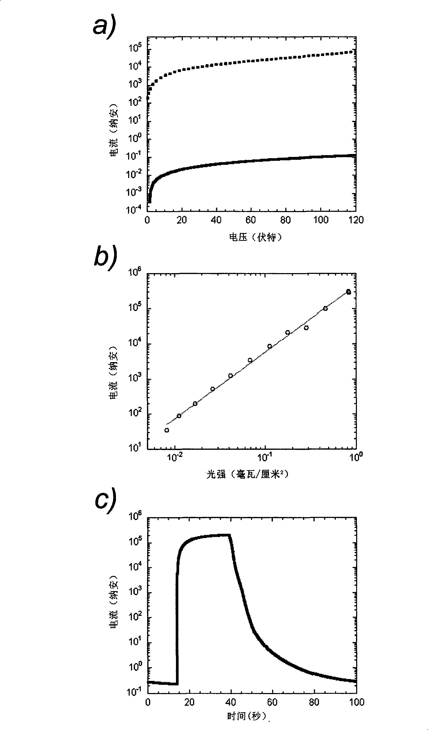
[0020] Dissolving ZnO nanocrystals in chloroform solvent to prepare a nanocrystal solution with a concentration of 50 mg / ml. The ZnO nanocrystal solution was spin-coated on the cleaned glass substrate by a spin-coating method to form a uniform film with a thickness of 100 nm. After annealing at 250°C for 20 minutes in air, a pair of T-shaped Ag electrodes with a spacing of 240 μm, a length of 3 mm, and a thickness of 60 nm were evaporated on the surface of the nanocrystalline film to prepare a nanocrystalline film device for ultraviolet detection. . For the test results of the device see figure 1 , with the following characteristics:

[0021] A. The dark current is extremely low, and the resistance at room temperature exceeds 1T (10 12 )Ω.

[0022] B. No response to light with a wavelength exceeding 400nm, that is, in the visible / infrared region.

[0023] C. The ultraviolet light guide has high sensitivity, at an intensity of 0.83mW / cm 2 Under the irradiation of 370nm ul...

Embodiment 2

[0028] The Mg-doped ZnO nanocrystals were dissolved in tetrahydrofuran solvent to prepare a nanocrystal solution with a concentration of 2 mg / ml. The ZnO nanocrystal solution was spin-coated on the cleaned SiO surface by spin coating method. 2 / Si substrate, a uniform thin film with a thickness of 10 nm was formed. After annealing at 350°C for 10 minutes in air, a pair of T-shaped Au electrodes with a distance of 240 μm, a length of 3 mm, and a thickness of 30 nm were evaporated on the surface of the nanocrystalline film to prepare a nanocrystalline film device for ultraviolet detection. .

Embodiment 3

[0030] Al-doped ZnO nanocrystals were dissolved in chloroform solvent to prepare a nanocrystal solution with a concentration of 100 mg / ml. The ZnO nanocrystal solution was spin-coated on the cleaned Si substrate by a spin-coating method to form a uniform film with a thickness of 200 nm. After annealing at 250°C for 30 minutes in air, a pair of T-shaped Cu electrodes with a distance of 240 μm, a length of 3 mm, and a thickness of 60 nm were evaporated on the surface of the nanocrystalline film to obtain a prototype of the ultraviolet detector. Nanocrystalline thin film devices used in ultraviolet detectors were prepared.


PUM

PropertyMeasurementUnit
Thicknessaaaaaaaaaa
Thicknessaaaaaaaaaa
Thicknessaaaaaaaaaa

Abstract

The present invention discloses a manufacturing method of a nanocrystalline thin-film device for ultraviolet detecting, which includes: the soluble semi-conductor nanocrystalline material is dissolved into the solvent to obtain nanocrystalline solution; the nanocrystalline solution is on the substrate by using the spin-coating method or jet ink print method to form a homogeneous nanocrystalline thin film; the nanocrystalline thin film is proceed annealing treatment about 10-60 minutes at the temperature 100-350EDG C, then vapor plating electric pole on the nanocrystalline thin film. The method of the present invention compared with the semiconductor film ultraviolet detector of traditional gas-phase high-temperature growth can reduce the cost of the ultraviolet detecting optoelectronic device without a vacuum device, low film build temperature, simple preparation technique, and can develop the ''flexibility device''of the large size flexible device. Because nanocrystalline has super large surface area, the nanocrystalline thin-film device for ultraviolet detecting has the features of low dark current and high sensitivity, etc.

Description

technical field [0001] The invention relates to a preparation method of a nanocrystalline thin film device for ultraviolet detection, in particular to a method for preparing a nanocrystalline thin film device for ultraviolet detection by a solution process. Background technique [0002] Ultraviolet detectors refer to devices that detect the presence and intensity of ultraviolet light, that is, electromagnetic waves with wavelengths between 400 and 10 nm. Ultraviolet light exists widely in nature and in production and life, and interacts with many substances. From fire alarm under weak light source, to aerial remote sensing monitoring of air pollution and space detection in high-energy physics research; from photomodification of organic polymers, to purification and disinfection of water sources or air, and medical cell detection and disease diagnosis ; From satellite ultraviolet communication, to military photoelectric countermeasures and infrared / ultraviolet dual-band guid...

Claims


Application Information

Patent Timeline
IPC IPC(8): H01L31/18
CPCY02P70/50
Inventor 金一政
Owner ZHEJIANG UNIV
Why Eureka
Try Eureka