Quanta amplified p type quanta trap infrared detector

An infrared detector and quantum well technology, applied in semiconductor devices, electrical components, circuits, etc., can solve the problems of low quantum efficiency and detection rate of devices, large effective mass of holes, low mobility, etc., and achieve high quantum efficiency and Responsiveness, process compatibility, high responsivity effect

Inactive Publication Date: 2008-09-10
SHANGHAI INST OF TECHNICAL PHYSICS - CHINESE ACAD OF SCI
View PDF0 Cites 6 Cited by
  • Summary
  • Abstract
  • Description
  • Claims
  • Application Information

AI Technical Summary

Problems solved by technology

However, due to the large effective mass and low mobility of the holes, it is difficult to transmit through the electrode layer on the order of microns to form a photocurrent, so the quantum efficiency and detection rate of the device are very low.

Method used


Image

  • Quanta amplified p type quanta trap infrared detector
  • Quanta amplified p type quanta trap infrared detector

Examples


Embodiment Construction

[0019] Below in conjunction with accompanying drawing and embodiment the specific embodiment of the present invention is described in further detail:

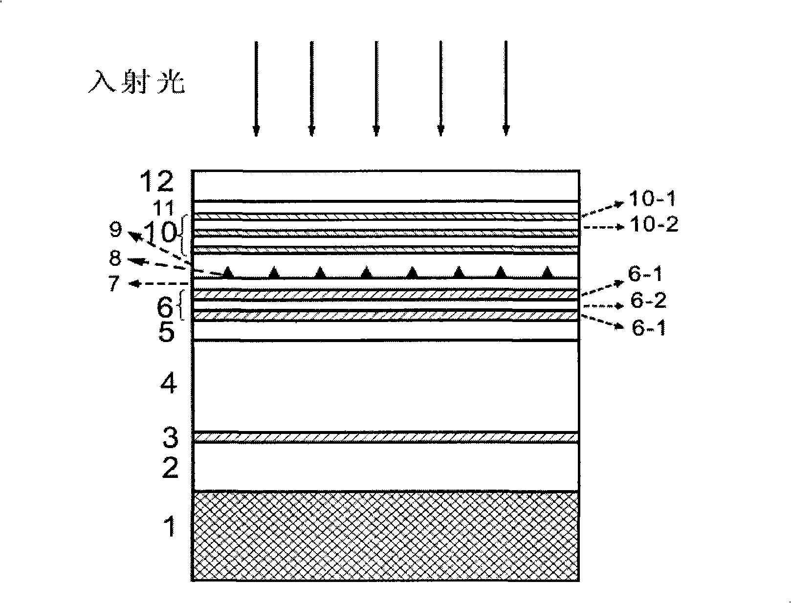
[0020] The p-type quantum well infrared detector structure of the quantum amplification of the present embodiment is as follows figure 1 shown. On the semi-insulating GaAs substrate 1, a 100-300nm GaAs buffer layer 2, an AlAs corrosion barrier layer 3, and n + GaAs lower electrode 4, first GaAs spacer layer 5, GaAs / AlGaAs double barrier layer 6, second GaAs spacer layer 7, InAs quantum dots 8, intrinsic GaAs quantum dot covering layers 9, 1 covering the InAs quantum dots -10 cycles of In y Ga 1-y As / GaAs quantum well active layer 10, third GaAs spacer layer 11, n + GaAs upper electrode layer 12 .

[0021] The thickness of the AlAs corrosion barrier layer 3 is determined by the process, generally below 20nm, preferably 10nm.

[0022] Gradient n + The thickness and doping concentration of the GaAs lower electrode layer 4 a...


PUM


Abstract

The invention discloses a p-type quantum well infrared detector with magnified quantum. The detector comprises a quantum dot resonant tunneling diode and a p-type quantum well active layer and is characterized in that the p-type quantum well active layer is integrated on an overburden layer of an intrinsic GaAs quantum dot of the quantum dot resonant tunneling diode. The detector adopts the core mechanism that the p-type quantum well active layer is utilized to absorb medium wave and long wave infrared and holes produced are captured by quantum dots close to a double barrier of the resonant tunneling diode; resonant tunneling current is changed intensively so as to cause the device of the invention to have both high quantum amplified factor of the quantum dot resonant tunneling diode and the response capability of normal incidence infrared wave band of the p-type quantum well infrared detector, thus overcoming the two key problems that restrain the application performance of the quantum well infrared detector, namely, normal incidence abstention and low quantum efficiency.

Description

technical field [0001] The invention relates to a p-type quantum well infrared detector, in particular to a p-type quantum well infrared detector for quantum dot resonant tunneling diode-assisted quantum amplification for detecting medium waves (3-5um) and long waves (8-12um) detector. Background technique [0002] Quantum well infrared detector (QWIP) has developed rapidly in the past ten years, and the development process from single device to focal plane device has been quite perfect. Among them, the n-type quantum well infrared detector (n-QWIP) has been extensively studied because of its small effective mass and high mobility, and the device has a high detection rate and response rate to infrared radiation. However, n-QWIP is limited by the selection rule of quantum transitions, so it is necessary to use dielectric or metal coupling gratings to absorb normal incident light, which brings great difficulties to the fabrication process of focal plane devices. For p-type q...

Claims


Application Information

Patent Timeline
Patent Type & Authority Applications(China)
IPC IPC(8): H01L31/111
Inventor 陆卫王旺平侯颖李天信陈平平张波甄红楼李宁陈效双
Owner SHANGHAI INST OF TECHNICAL PHYSICS - CHINESE ACAD OF SCI
Why Eureka
Try Eureka