Fabricating method for semiconductor device

A manufacturing method and semiconductor technology, applied in semiconductor/solid-state device manufacturing, electrical components, circuits, etc., can solve problems such as complexity and reduce the PMOS gate manufacturing process, and achieve the effect of simple process steps

Active Publication Date: 2008-10-29
SEMICON MFG INT (SHANGHAI) CORP +1
View PDF2 Cites 9 Cited by
  • Summary
  • Abstract
  • Description
  • Claims
  • Application Information

AI Technical Summary

Problems solved by technology

[0013] The above method of etching back polysilicon to reduce the thickness of the PMOS gate to form gates with different thicknesses has a relatively complicated manufacturing process.

Method used


Image

  • Fabricating method for semiconductor device
  • Fabricating method for semiconductor device
  • Fabricating method for semiconductor device

Examples


Embodiment Construction

[0070] The specific embodiments of the present invention will be described in detail below in conjunction with the accompanying drawings.

[0071] Figure 8 It is a flow chart of an embodiment of the manufacturing method of the semiconductor device of the present invention.

[0072] Such as Figure 8 The flow chart shown, step S100, provides a semiconductor substrate having a first region and a second region.

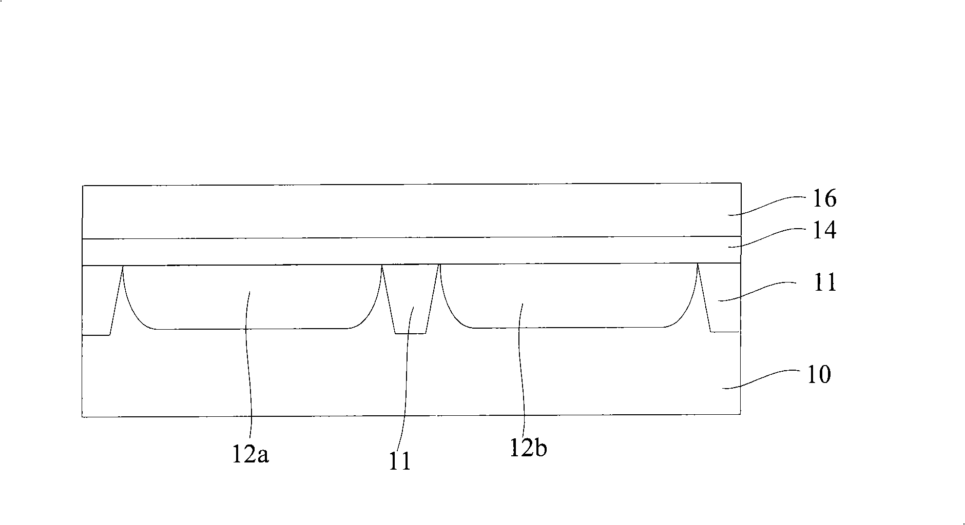
[0073] Such as Figure 9 The schematic cross-sectional view shown provides a semiconductor substrate 30 having a first region 30a and a second region 30b. The material of the semiconductor substrate 30 can be one of monocrystalline silicon, polycrystalline silicon, and amorphous silicon, the material of the semiconductor substrate 30 can also be a silicon-germanium compound, and the semiconductor substrate 30 can also be an insulating layer. Silicon (Silicon On Insulator, SOI) structure or epitaxial layer structure on silicon. N-type impurities or P-type impurities...


PUM


Abstract

A manufacture method for a semiconductor apparatus includes the following steps of: providing a semiconductor underlay with a first area and a second area; forming polysilicon layers on the semiconductor underlay; reducing the thickness of the polysilicon layer of the second area to lead the thickness of the polysilicon layer of the second area to be less than that of the first area; patterning the polysilicon layers of the first area and the second area; forming a first grid in the first area and forming a second grid in the second area. The technique of manufacturing the grids with different thicknesses of the method is simpler.

Description

technical field [0001] The invention relates to the technical field of semiconductor manufacturing, in particular to a manufacturing method of a semiconductor device. Background technique [0002] Complementary Metal-Oxide-Semiconductor (CMOS) devices are widely used in storage, communication, computer and other fields due to their low power consumption, high response rate and other characteristics. CMOS devices include NMOS transistors and PMOS transistors, and gate materials of the NMOS transistors and PMOS transistors are usually N-type doped or P-type doped polysilicon. Figure 1 to Figure 4 It is a schematic cross-sectional view of a structure corresponding to each step of an existing manufacturing method of a CMOS device. [0003] Such as figure 1 As shown, a shallow trench isolation 11, a P well 12a and an N well 12b are formed in a semiconductor substrate 10, the P well is used to form the conduction channel of the NMOS transistor, and the N well is used to form th...

Claims


Application Information

Patent Timeline
Patent Type & Authority Applications(China)
IPC IPC(8): H01L21/8234H01L21/8238
Inventor 张海洋陈海华黄怡朱峰
Owner SEMICON MFG INT (SHANGHAI) CORP
Why Eureka
Try Eureka