Organic light emitting device

A technology of organic light-emitting devices and light-emitting layers, which is applied in lighting devices, electroluminescent light sources, organic semiconductor devices, etc., and can solve the problems of unsatisfactory connection voltage, luminous efficiency, and life properties of organic light-emitting devices.

Active Publication Date: 2008-11-19
SAMSUNG DISPLAY CO LTD
View PDF3 Cites 34 Cited by
  • Summary
  • Abstract
  • Description
  • Claims
  • Application Information

AI Technical Summary

Problems solved by technology

[0006] Despite these advantages, the turn-on voltage, luminous efficiency, lifetime properties, etc. of conventional organic light-emitting devices are still unsatisfactory

Method used


Image

  • Organic light emitting device
  • Organic light emitting device
  • Organic light emitting device

Examples


Embodiment approach

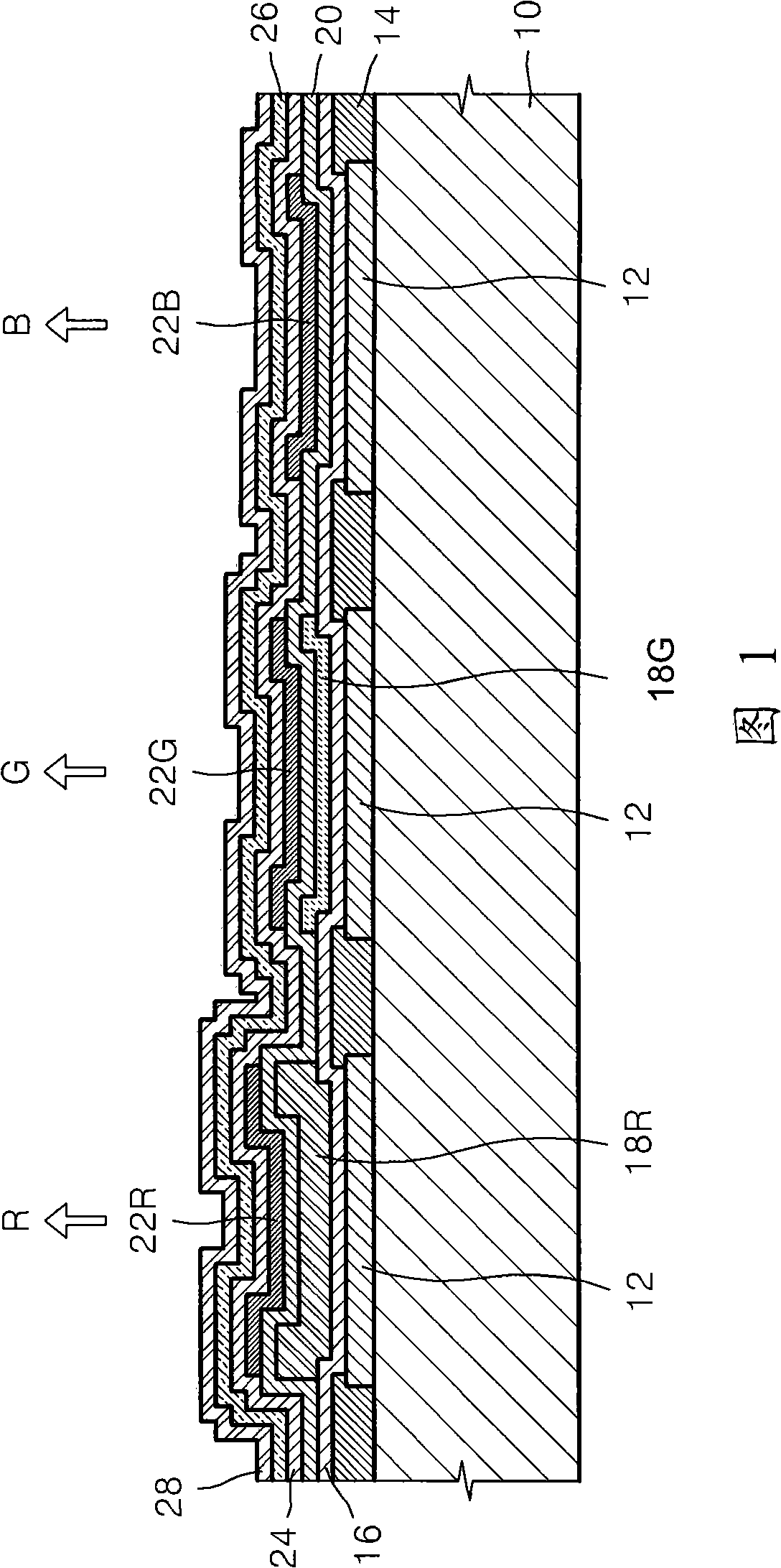
[0020] FIG. 1 is a schematic cross-sectional view of an organic light emitting device according to an embodiment of the present invention.

[0021] Referring to FIG. 1 , the organic light emitting device includes a substrate 10 , a first electrode 12 , a hole injection layer 16 and respectively patterned red light emitting layers 22R, green light emitting layers 22G and blue light emitting layers 22B. The first auxiliary layer 18R is disposed between the hole injection layer 16 and the red light emitting layer 22R to adjust the resonance period of red light. The second auxiliary layer 18G is disposed between the hole injection layer 16 and the green light emitting layer 22G to adjust the resonance period of green light. The hole transport layer 20 is arranged at the lower portion of the red light emitting layer 22R, the green light emitting layer 22G, and the blue light emitting layer 22B. The electron transport layer 24 , the electron injection layer 26 and the second electr...

Embodiment 1

[0081] 15Ω / cm 2 (1200 ) The ITO glass substrate was cut into a size of 50mm×50mm×0.7mm as an anode, and was washed with isopropanol and pure water by microwave for 5 minutes respectively. The ITO glass substrate was irradiated with ultraviolet rays for 30 minutes and washed with ozone, and then installed in a vacuum deposition apparatus.

[0082] A hole injection material (product name: LHT-001) purchased from LUDIS was vacuum deposited onto the glass substrate to form a hole injection layer with a thickness of 130 nm. Then, a hole transport material (product name: IDE-406) purchased from Idemitsu Corporation was vacuum-deposited to form a first auxiliary layer with a thickness of 80 nm. Then vacuum-deposit 4,4'-bis[N-(1-naphthyl)-N-phenylamino]biphenyl (NPB) on the first auxiliary layer to form a hole transport layer with a thickness of 20 nm.

[0083] Known red phosphorescent host material GDI1403 and known red phosphorescent dopant Ir(piq) available from Gracel 3 (dopi...

Embodiment 2

[0086] An organic light-emitting device was prepared in the same manner as in Example 1, except that HTM016 from Merck was used instead of IDE406 from Idemitsu in the process of forming the first auxiliary layer.


PUM

PropertyMeasurementUnit
thicknessaaaaaaaaaa
thicknessaaaaaaaaaa
thicknessaaaaaaaaaa

Abstract

Organic light emitting devices (OLEDs) are provided. An exemplary OLED includes a substrate, a first electrode, a second electrode, and an organic layer between the first and second electrodes having a hole injection layer and an emissive layer. The emissive layer includes red, green and blue emissive layers. The organic layer further includes an auxiliary layer selected from a first auxiliary layer between the hole injection layer and the red emissive layer for adjusting the resonance cycle of red light, a second auxiliary layer between the hole injection layer and the green emissive layer for adjusting the resonance cycle of green light, and combinations thereof. The material of the auxiliary layer is different from the material of the hole injection layer. The organic light emitting device has low turn-on voltage, high current density, high luminance, high current efficiency, high power, long life-time, and excellent color purity.

Description

[0001] Cross References to Related Applications [0002] This application claims the benefit of Korean Patent Application No. 10-2007-0047849 filed with the Korean Patent Office on May 16, 2007, the disclosure of which is hereby incorporated by reference in its entirety. technical field [0003] The present invention relates to an organic light-emitting device, in particular to an organic light-emitting device including an auxiliary layer to adjust the resonance period of red light and / or green light. The organic light emitting device has improved electrical properties such as turn-on voltage, efficiency, lifetime, and the like. Background technique [0004] An organic light emitting device (OLED), which is a self-emitting device, has a wide viewing angle, excellent contrast, fast response time, good operating voltage, and is capable of multicolor images. Therefore, a great deal of research on OLEDs for various commercial applications has been conducted. [0005] Generally...

Claims


Application Information

Patent Timeline
Patent Type & Authority Applications(China)
IPC IPC(8): H01L27/32H01L51/50H01L51/54
CPCH01L51/5096H01L51/0078H01L51/0059H01L51/0037H01L27/3211H01L51/5265H01L51/5048H01L2251/558H01L51/5088H01L51/0035H10K59/35H10K85/111H10K85/1135H10K85/631H10K85/311H10K50/14H10K50/18H10K50/17H10K50/852H10K2102/351H05B33/22H05B33/20
Inventor 千民承李宽熙金美更金东宪郭在见孙正河
Owner SAMSUNG DISPLAY CO LTD
Why Eureka
Try Eureka