

Preparation method of high-temperature superconductor nano-structured array
A nanostructure, high-temperature superconducting thin film technology, applied in the direction of nanostructure manufacturing, superconductor element usage, superconducting/high-conducting conductors, etc., can solve the problems of serious diffusion and the inability to directly prepare high-temperature superconducting thin films, etc. The effect of growth control
- Summary
- Abstract
- Description
- Claims
- Application Information
AI Technical Summary
Problems solved by technology
Method used
Image

Examples
Embodiment 1
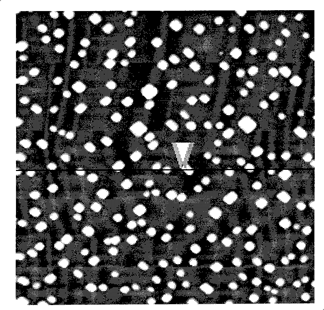
[0028] 1) CeO on sapphire 2 Fabrication of buffer layer nanostructures
[0029] ① Deposition: using pulsed laser deposition method on the R surface sapphire [Al 2 o 3 (1 1 02)] CeO growth on single crystal substrate 2 buffer layer ultra-thin film; the CeO 2 The film deposition rate was 0.05 nm per laser pulse, the CeO 2 The thickness of the film is controlled at 2nm, and the prepared CeO 2 Film samples are "as-grown" film samples;
[0030] ②Annealing: The "grown" thin film sample is introduced into the annealing chamber under (ultra) high vacuum, flowed with oxygen, annealed in situ at 1050°C for 60 minutes, and then cooled to room temperature to obtain CeO 2 a substrate for a nanostructured buffer layer;
[0031] 2) Interfacial self-assembly growth of nanostructures of YBCO high temperature superconducting materials
[0032] ① Deposition: then with CeO 2 The sapphire substrate of the nanostructure buffer layer is introduced into the pulsed laser deposition cavity un...
Embodiment 2
[0041] 1) CeO on sapphire 2 Fabrication of buffer layer nanostructures
[0042] ① Deposition: using pulsed laser deposition method on the R surface sapphire [Al 2 o 3 (1 1 02)] CeO growth on single crystal substrate 2 buffer layer ultra-thin film; the CeO 2 The film deposition rate was 0.02 nm per laser pulse, the CeO 2 The thickness of the film is controlled at 10nm, and the prepared CeO 2 Film samples are "as-grown" film samples;
[0043] ②Annealing: The "grown" thin film sample is introduced into the annealing chamber under (ultra) high vacuum, flowed with oxygen, annealed in situ at 1400°C for 10 minutes, and then cooled to room temperature to obtain CeO 2 a substrate for a nanostructured buffer layer;
[0044] 2) Interfacial white assembly growth of nanostructures of YBCO high temperature superconducting materials
[0045] ① Deposition: then with CeO 2 The sapphire substrate of the nanostructure buffer layer is introduced into the pulsed laser deposition cavity ...
Embodiment 3
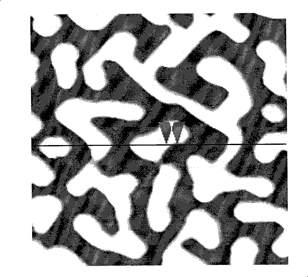
[0054] 1) Preparation of nanostructure of YSZ buffer layer on sapphire
[0055] ① Deposition: using pulsed laser deposition method on the R surface sapphire [Al 2 o 3 (1 1 02)] growing a YSZ buffer layer ultra-thin film on a single crystal substrate; the deposition rate of the YSZ film is 0.04nm per laser pulse, and the thickness of the YSZ film is controlled at 10nm, and the prepared CeO 2 Film samples are "as-grown" film samples;
[0056] ②Annealing: Put the "grown" thin film sample into the fiber resistance furnace, introduce flowing oxygen, anneal at 1250°C for 30 minutes, and then cool to room temperature to prepare a substrate with a YSZ nanostructure buffer layer;
[0057] 2) Interfacial self-assembly growth of nanostructures of YBCO high temperature superconducting materials
[0058] ① Deposition: Utilize the pulsed laser deposition method to grow a YBCO high temperature superconducting material film on a sapphire substrate with a YSZ nanostructure buffer layer; th...
PUM
| Property | Measurement | Unit |
|---|---|---|
| thickness | aaaaa | aaaaa |
| thickness | aaaaa | aaaaa |
| wavelength | aaaaa | aaaaa |
Abstract
Description
Claims
Application Information