Thin-film transistor array substrate and preparation method thereof

A technology of thin film transistors and array substrates, which is applied in the field of thin film transistor array substrates with photosensors and its production, can solve problems such as photocurrent attenuation and affect the reliability of photosensors, and achieve cost savings, improved photocurrent characteristics, The effect of increasing the production cost

Active Publication Date: 2008-12-17
AU OPTRONICS CORP
View PDF0 Cites 26 Cited by
  • Summary
  • Abstract
  • Description
  • Claims
  • Application Information

AI Technical Summary

Problems solved by technology

[0005] However, when the amorphous silicon material is used as the light sensing material of the photosensor, the following problem is faced: even if no voltage is applied to the electrodes on both sides of the amorphous silicon, as long as the amorphous silicon material is irradiated by light, the photosensor will generate The problem of photocurrent attenuation affects the reliability of the photosensor

Method used


Image

  • Thin-film transistor array substrate and preparation method thereof
  • Thin-film transistor array substrate and preparation method thereof
  • Thin-film transistor array substrate and preparation method thereof

Examples


Embodiment Construction

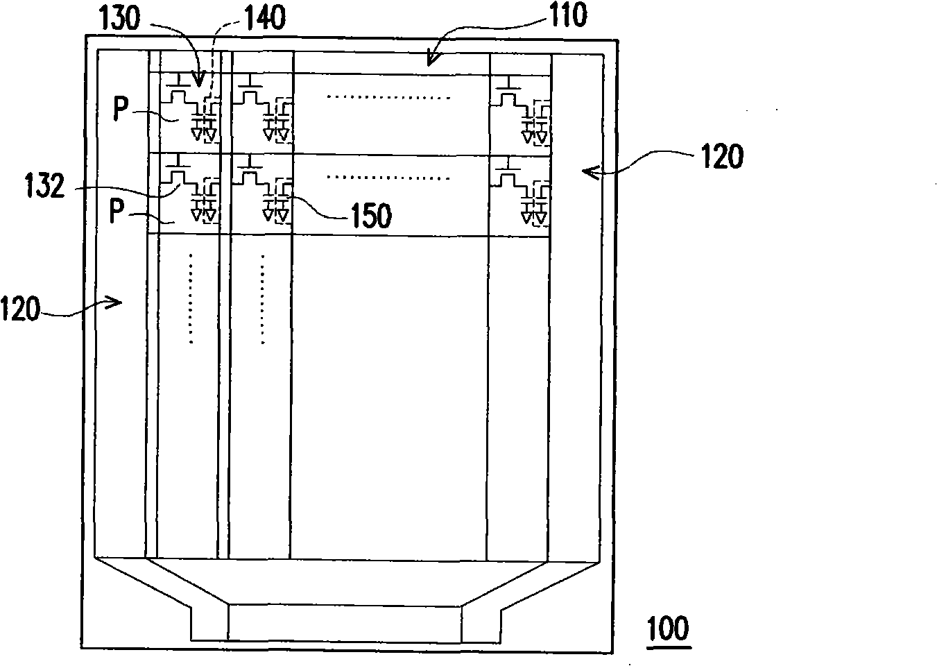
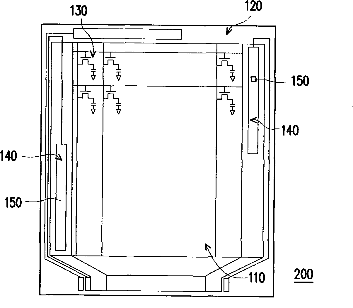
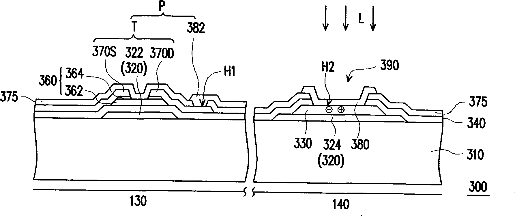
[0075] Please refer to Figure 1A and Figure 1B , which respectively illustrate the layout of a thin film transistor array substrate integrated with photosensors according to an embodiment of the present invention. Please refer to Figure 1A The thin film transistor array substrate 100 at least has a display area 110 and a peripheral circuit area 120 located on the periphery of the display area 110 . The display area 110 has a plurality of pixel areas 130 arranged in an array. When the TFT array substrate 100 is applied to a liquid crystal display, the plurality of pixel units P in the pixel area 130 are used to display a frame. Driving components such as scan drivers or data drivers (not shown) can be arranged in the peripheral circuit area 120 . The light sensing area 140 is used to configure the light sensor 150 , and the light sensing area 140 can be designed at different positions on the TFT array substrate 100 according to different application levels.

[0076] For m...


PUM

PropertyMeasurementUnit
minimum film forming temperatureaaaaaaaaaa
refractive indexaaaaaaaaaa

Abstract

The invention discloses a thin-film transistor array substrate and a manufacturing method thereof. The method comprises the following steps of: (1) providing a substrate with a pixel region and a light sensing region; (2) forming a first patterned conducting layer on the substrate, wherein the first patterned conducting layer comprises a grid electrode positioned in the pixel region and a first electrode positioned in the light sensing region, and forming a light sensing dielectric layer on the first electrode; (3) forming a grid electrode insulating layer on the substrate to cover the grid electrode, the light sensing dielectric layer and the first electrode; (4) forming a patterned semiconductor layer on the grid electrode insulating layer above the grid electrode; (5) forming a source electrode and a drain electrode on the patterned semiconductor layer at two sides of the grid electrode, wherein the grid electrode, the source electrode and the drain electrode form a thin-film transistor; and (6) forming a second electrode on the light sensing dielectric layer.

Description

technical field [0001] The present invention relates to a thin film transistor array substrate and a manufacturing method thereof, in particular to a thin film transistor array substrate with a light sensor and a manufacturing method thereof. Background technique [0002] With the advancement of technology, the technology of the display is also constantly developing and its demand is increasing day by day. In the early days, due to the excellent display quality and technical maturity of the cathode ray tube (Cathode Ray Tube, CRT), it monopolized the display market for many years. However, due to the rise of the concept of green environmental protection recently, based on the characteristics of large energy consumption and large radiation generated by cathode ray tubes, and the limited space for flattening their products, cathode ray tubes cannot meet the market demand for light, thin, short , small, beautiful and low power consumption market trends. Therefore, the thin an...

Claims


Application Information

Patent Timeline
Patent Type & Authority Applications(China)
IPC IPC(8): H01L21/84H01L27/144G02F1/1362G06F3/042
Inventor 李明贤石靖节卓恩宗彭佳添林昆志
Owner AU OPTRONICS CORP
Why Eureka
Try Eureka