

Semiconductor electrode, preparation method thereof and solar cell comprising semiconductor electrode
A technology of solar cells and semiconductors, applied in the field of dye-sensitized solar cells, can solve the problems of low conductivity of nano titanium dioxide layer, low photoelectric conversion rate of dye-sensitized solar cells, etc.
- Summary
- Abstract
- Description
- Claims
- Application Information
AI Technical Summary
Problems solved by technology
Method used
Image

Examples
preparation example Construction
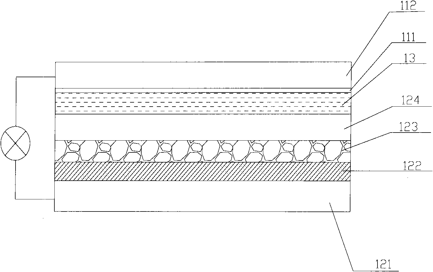
[0018] The preparation method of the semiconductor electrode provided by the invention comprises forming a dense semiconductor layer containing semiconductor particles and conductive particles on the conductive bottom layer, and then forming a porous semiconductor layer containing semiconductor particles and conductive particles on the dense semiconductor layer, and then A dye layer is formed on the porous semiconductor layer, wherein the conductive particles are metal or alloy particles selected from one or more of Au, Ag, Pt, Cu, Zn, Sn, Ni, Fe, Ir, Ru and In , the weight ratio of semiconductor particles to conductive particles in the dense semiconductor layer is 100-200:1-2.
[0019] The dense semiconductor layer is a co-deposition layer prepared by a co-deposition method. The preparation method includes using platinum as an anode and a conductive bottom layer as a cathode. The co-deposition solution includes an aqueous solution of semiconductor particles, water-soluble meta...
Embodiment 1
[0040] This example is used to prepare the semiconductor electrode for a dye-sensitized solar cell provided by the present invention and the dye-sensitized solar cell containing the semiconductor electrode.
[0041] (1) Preparation of co-deposition solution
[0042] Disperse 1 gram of titanium dioxide particles (particle diameter 15 nm) uniformly into 5 ml of 50% aqueous solution of isopropanol, 0.1 ml of acetylacetone, and then add 0.01 g of AgNO 3 , the pH value is 6 and the stirring is continued for 20 minutes to obtain the co-deposition solution P1.
[0043] (2) Preparation of dense semiconductor layer
[0044] Use the platinum sheet as the anode, on the conductive glass coated with fluorine-doped tin dioxide layer with a size of 3 × 1.5 cm (FTO conductive glass with a square resistance of 15 ohms manufactured by Qinhuangdao Yaohua Glass Co., Ltd., with a thickness of 4 mm) , as the cathode, the co-deposition solution is P1, and the dense semiconductor layer A1 can be ob...
Embodiment 2
[0055] This example is used to prepare the semiconductor electrode for dye-sensitized solar cell provided by the present invention and the dye-sensitized solar cell containing the semiconductor electrode.
[0056]Dye-sensitized solar cell R2 was prepared in the same manner as in Example 1, except that co-deposition solution P2 was used instead of co-deposition solution P1 when preparing the dense semiconductor layer, and semiconductor slurry D2 was used instead of semiconductor solution P1 when preparing the porous semiconductor layer. Serum D1.
[0057] 2 grams of TiO2 powder (particle diameter is 23 nanometers) is evenly dispersed into 10 milliliters, the concentration is 70% ethanol aqueous solution, 0.2 milliliters of acetylacetone, then add 0.025g CuSO4, keep stirring for 1 hour, can obtain coprecipitation solution P2.
[0058] Mix metal copper particles (particle diameter is 20 nanometers), nano-titanium dioxide semiconductor particles, polyethylene glycol, OP-10, and ac...
PUM
| Property | Measurement | Unit |
|---|---|---|
| Diameter | aaaaa | aaaaa |
| Thickness | aaaaa | aaaaa |
| Thickness | aaaaa | aaaaa |
Abstract
Description
Claims
Application Information